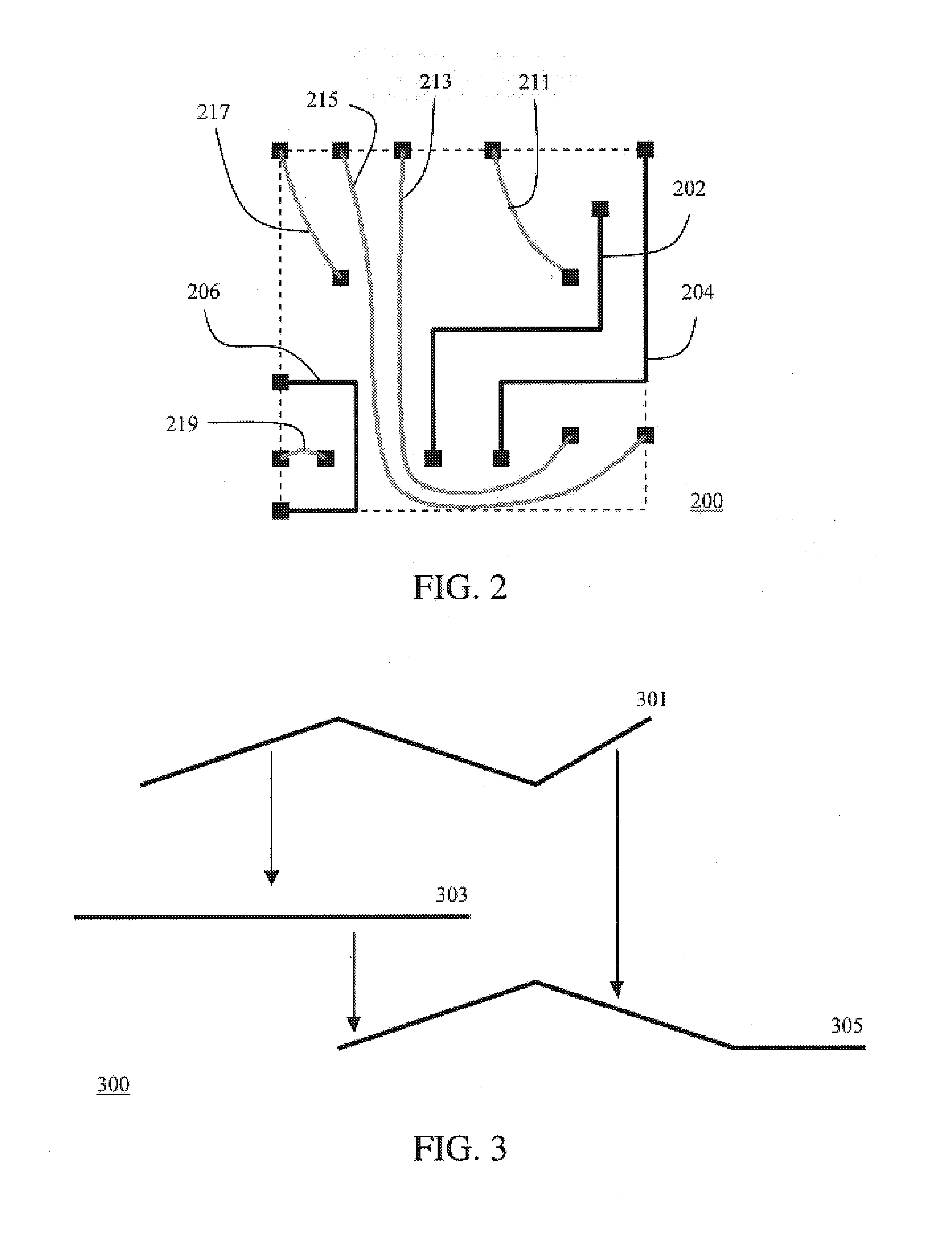
Wire spreading through geotopological layout
a geotopological layout and wire technology, applied in the field of automatic layout optimization tools, can solve the problems of bridging faults, affecting the design, and affecting the overall design, so as to reduce crosstalk noise, reduce metal fills, and reduce particle related yield loss
- Summary
- Abstract
- Description
- Claims
- Application Information
AI Technical Summary
Benefits of technology
Problems solved by technology
Method used
Image

Examples
Embodiment Construction
[0032]In the following detailed description, like numbers / characters may be used to refer to identical, corresponding, or similar items in different figures.
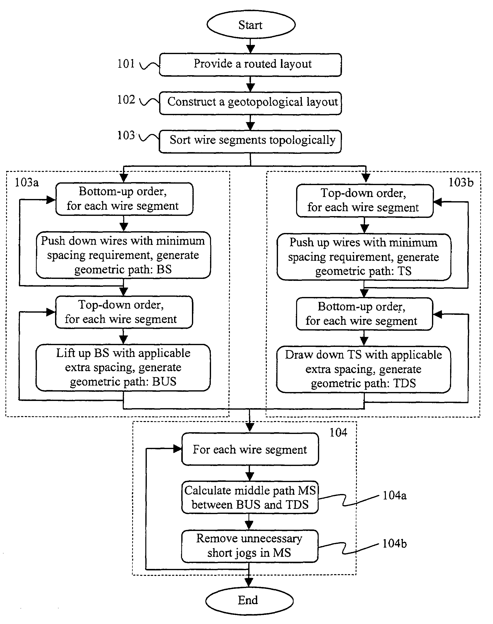
[0033]The present invention provides a computer-implemented layout optimization tool with an innovative wire spreading tool useful in reducing yield loss, crosstalk, metal fill, power consumption, among others. Based on a preferred geotopological layout optimization flow, this invention increases wire-to-wire spacing in a post-routing layout, effectively achieving full layout wire spreading without creating any design rule violations in the layout.
[0034]The geotopological layout optimization flow has many advantages over geometry-based and topology-based methods of layout optimization flow. As an example, a conventional layout optimization flow generally follows a topological approach in which a topological layout is first extracted from a geometrical layout. Specified layout modifications, such as wiring sizing and spacing or r...
PUM
 Abstract
Description
Claims
Application Information
 - R&D
- Intellectual Property
- Life Sciences
- Materials
- Tech Scout
- Unparalleled Data Quality
- Higher Quality Content
- 60% Fewer Hallucinations
Browse by: Latest US Patents, China's latest patents, Technical Efficacy Thesaurus, Application Domain, Technology Topic, Popular Technical Reports.
© 2025 PatSnap. All rights reserved.Legal|Privacy policy|Modern Slavery Act Transparency Statement|Sitemap|About US| Contact US: help@patsnap.com