
Treated copper foil and circuit board

a technology of copper foil and circuit board, applied in the direction of insulating substrate metal adhesion improvement, core/yoke, transportation and packaging, etc., can solve the problems of low hygroscopicity, low peel strength, and low hygroscopicity, and achieve low hygroscopicity and low cost. , the effect of low cos

Inactive Publication Date: 2008-06-03
FURUKAWA ELECTRIC CO LTD
View PDF10 Cites 24 Cited by
  • Summary
  • Abstract
  • Description
  • Claims
  • Application Information

AI Technical Summary

Benefits of technology

The present invention provides a treated copper foil that can form fine patterns and has high peel strength. The foil can be used with general epoxy resin, polyimide films, and mesomorphic polymers that have low hygroscopicity and can withstand soldering. The treated copper foil has a roughening treated surface with specific surface roughness and projections. The circuit board formed using this foil has better high frequency properties. The treated copper foil is deposited with roughening particles on at least one side of the copper foil, which makes a surface roughness of not more than -30. The roughening particles are made of copper or copper alloy and are distributed in a specific pattern. The surface roughness of the untreated copper foil before roughening treatment is not more than 2 μm. The treated copper foil can be coated with a film of Ni or Ni alloy, a stainproof layer of Zn or Zn alloy and / or Cr metal or chromate, or a silane coupling layer. The technical effects of this invention are improved peeling strength, fine pattern formation, and high frequency performance of the treated copper foil and circuit board.

Problems solved by technology

However, dielectric property of polyimide changes greatly with absorption of moisture and also high frequency property drops greatly in humid environment.
As a result, the process becomes complicated.
However, copper film has a low peel strength with mesomorphic polymer compared with polyimide.
Among epoxy resins, polyimide resins, and mesomorphic polymers, mesomorphic polymers are known to be poor in peel strength with copper foil.
It is true that this method is suitable for improving peel strength, but, for high frequency property, in terms of surface effect, it is not preferable to increase the surface roughness Rz and the amount of roughening particles.
Depending on the type of mesomorphic polymer resin, the increased surface roughness Rz dose not always improve the peel strength.
Improving the peel strength by raising the surface roughness Rz by roughening particles or increasing the amount of deposition is not suitable when forming such fine patterns.
It is also possible to roughen the surface of untreated copper foil and reduce the amount of deposition of roughening particles to improve the peel strength, but this is not suitable for obtaining a high frequency property and producing fine patterns.
With non-roughened copper foil, the mesomorphic polymer film is easily destroyed at just underneath the boundary with copper foil, so the desired peel strength cannot be obtained.
Even with such methods, however, not enough peel strength is obtained with copper foil having low surface roughness.

Method used


Image

  • Treated copper foil and circuit board
  • Treated copper foil and circuit board
  • Treated copper foil and circuit board

Examples


examples

[0076]Below, the present invention will be explained in detail with reference to specific examples, but the present invention is not limited to these examples.

[0077]In these examples, the following copper foils, treatment plating solutions, and insulation board films were used.

[0078]Copper Foils

[0079]Original Copper Foil 1: Untreated electrodeposited and rolled copper foil with thicknesses of 12 μm, matte side roughnesses Rz of 1.26 μm, and shiny side roughnesses Rz of 1.82 μm were prepared.

[0080]Original Copper Foil 2: Untreated electrodeposited and rolled copper foil with thicknesses of 12 μm, matte side roughnesses Rz of 1.52 μm, and shiny side roughnesses Rz of 1.46 μm were prepared.

[0081]Original Copper Foil 3: Untreated electrodeposited and rolled copper foil with thicknesses of 12 μm, matte side roughnesses Rz of 1.86 μm, and shiny side roughnesses Rz of 1.2 μm were prepared.

[0082]Treatment Plating Solutions and Plating Conditions

[0083]Electroplating A[0084]Plating Bath 1[008...


PUM

PropertyMeasurementUnit
surface roughness Rzaaaaaaaaaa
heightaaaaaaaaaa
heightaaaaaaaaaa

Abstract

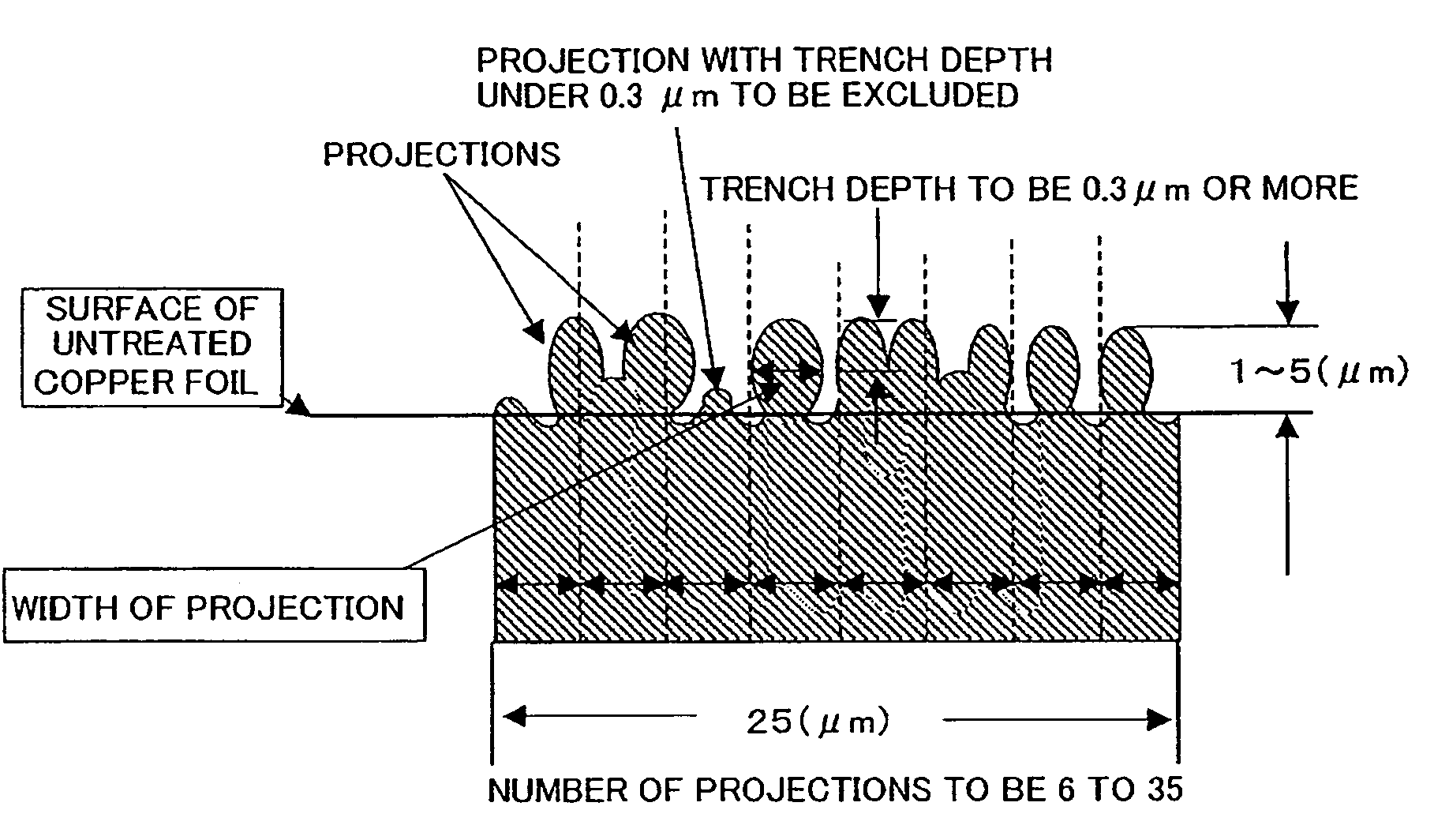
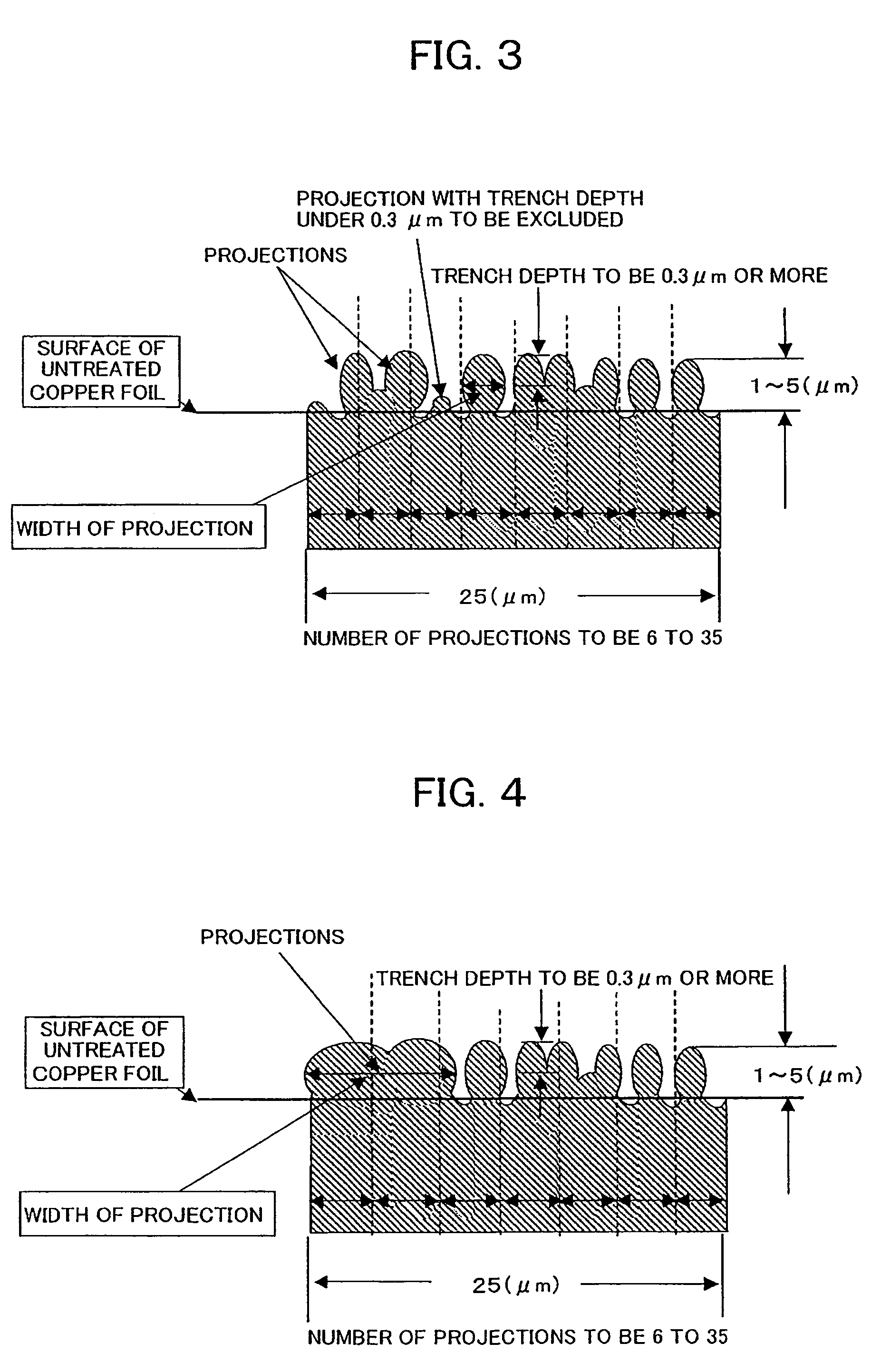
An object of the present invention is to provide a treated copper foil laminated with a mesomorphic polymer film having low hygroscopicity and superior high thermal resistance to make a circuit board composite materials having large peel strength and compatibility with fine pattern processes, which a copper foil being deposited with roughening particles to make the treated copper foil having a roughening treated side with surface roughness of 1.5 to 4.0 μm and luminosity of not more than 30, having projections formed from the roughening particles with a height of 1 to 5 μm, preferably 6 to 35 thereof are uniformly distributed in a 25 μm of surface length of copper foil cross-section observed, and its maximum width being at least 0.01 μm and not more than twice of 25 μm divided by the number of projections in the 25 μm surface length.

Description

BACKGROUND OF THE INVENTION[0001]1. Field of the Invention[0002]The present invention relates to a treated copper foil improved in peel strength with epoxy resin, polyimide resin, or thermoplastic mesomorphic polymer-based film (hereinafter called “mesomorphic polymer film”), more particularly relates to a treated copper foil laminated with such films for flexible board, high density mount multilayer board, or high frequency circuit board and to a circuit board formed by using the treated copper foil.[0003]2. Description of the Related Art[0004]The recent demand for increasing smaller size and lighter weight of electronic equipments have led to highly integrated electronic components. A composite circuit board for producing flexible board, high density mount multilayer board, high frequency circuit board, etc. used for the above components (hereinafter called “circuit board”) consists of conductors (copper foil) and insulator boards to support the conductors. The insulator board sec...

Claims


Application Information

Patent Timeline
Patent Type & Authority Patents(United States)
IPC IPC(8): B32B15/20C25D1/04H05K3/38
CPCC25D1/04H05K3/384H05K2201/0355H05K2203/0307H05K2203/0723Y10T428/1291Y10T428/25Y10T428/24917Y10T428/12063Y10T428/12993Y10T428/12438Y10T428/12903C25D7/0614C25D5/627C25D5/605H05K1/09H05K3/38
Inventor SUZUKI, YUUJI
Owner FURUKAWA ELECTRIC CO LTD
Learn More