Method of forming exposure mask pattern, exposure mask pattern, and method of producing semiconductor device

a technology of exposure mask and pattern, which is applied in the direction of photomechanical equipment, originals for photomechanical treatment, instruments, etc., can solve the problem that the direction of extension of the facing side cannot be arranged in step manner, and the edge division points given inside the design pattern can be prevented, the number of exposure shots can be reduced, and the amount of data of the exposure mask can be reduced.

Inactive Publication Date: 2008-06-10
SONY CORP
View PDF9 Cites 23 Cited by
  • Summary
  • Abstract
  • Description
  • Claims
  • Application Information

AI Technical Summary

Benefits of technology

[0012]In the above method of forming an exposure mask pattern, exposure mask pattern, and method of producing a semiconductor device, since edge division points are set at facing sides of a rectangular pattern by predetermined intervals from two vertexes sharing one side of the rectangular pattern, the edge division points are provided at the facing sides with no “deviation” in the direction of extension of the facing sides. Therefore, when correcting the edge positions in the edge portions divided by the edge division points, the corrected edge portions cannot be arranged in the direction of extension of the facing sides in a step manner. Accordingly, when dividing an exposure mask pattern obtained by the above correction in the direction of extension of the facing sides to divide it into rectangular divided pattern portions, the interval between the edge division points becomes the minimum unit of division and the number of the rectangular divided patterns is kept to no more than the number of portions between the edge division points. Due to this, the shape of the exposure mask pattern is simplified, guarantee of the mask against defects becomes easy, and a transfer pattern having a high precision with respect to the design pattern can be formed. Note that the above rectangular pattern may be a rectangle or a square. Further, the interval of provision of the division points may be a constant value.
[0013]In the step of forming the rectangular patterns, by making portions of the design pattern having a distance between the facing sides within a predetermined interval the rectangular patterns, in a long pattern having a bent part, the rectangular patterns are formed at portions other than the pattern comprising the bent part. Therefore, when providing the edge division points at the facing sides of the rectangular patterns, edge division points being given inside the design pattern can be prevented.
[0015]Further, according to the method of producing a semiconductor device performing pattern exposure of an exposure mask pattern obtained in this way, when dividing an exposure mask pattern obtained by the above correction in the direction of extension of the facing sides to divide it into rectangular divided patterns, the interval between the edge division points becomes the minimum unit of division, the number of the rectangular divided patterns is kept to no more than the number of portions between the edge division points, an increase of the number of the mask data and the number of the exposure shots when producing a mask, and deterioration of the TAT (turn-around time) due to this can be prevented.
[0016]Further, in this method of producing a semiconductor device, when the pattern exposure is performed using an exposure mask having exposure mask patterns, the amount of data of the exposure mask can be reduced. On the other hand, when the pattern exposure is lithographic exposure, the number of the exposure shots can be reduced.
[0017]Further, if the pattern exposure is electron beam exposure, X-ray exposure, or photo exposure, in particular, for such pattern exposure using an exposure mask requiring fine patterns or high density patterns, an increase of the amount of the mask data and the number of shots in the pattern exposure when producing the mask and deterioration of the TAT can be effectively prevented.

Problems solved by technology

Therefore, when correcting the edge positions in the edge portions divided by the edge division points, the corrected edge portions cannot be arranged in the direction of extension of the facing sides in a step manner.

Method used


Image

  • Method of forming exposure mask pattern, exposure mask pattern, and method of producing semiconductor device
  • Method of forming exposure mask pattern, exposure mask pattern, and method of producing semiconductor device
  • Method of forming exposure mask pattern, exposure mask pattern, and method of producing semiconductor device

Examples


Embodiment Construction

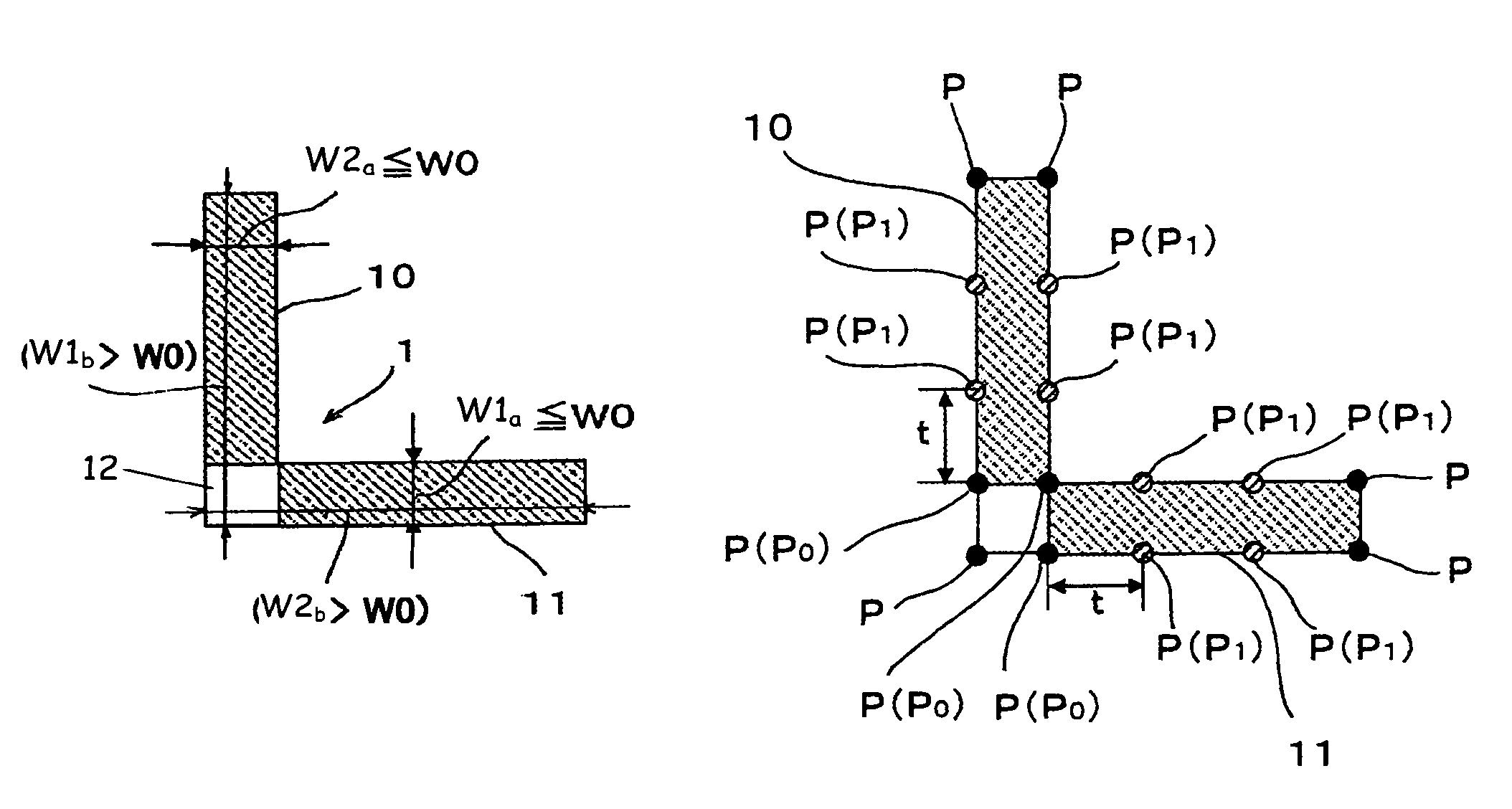
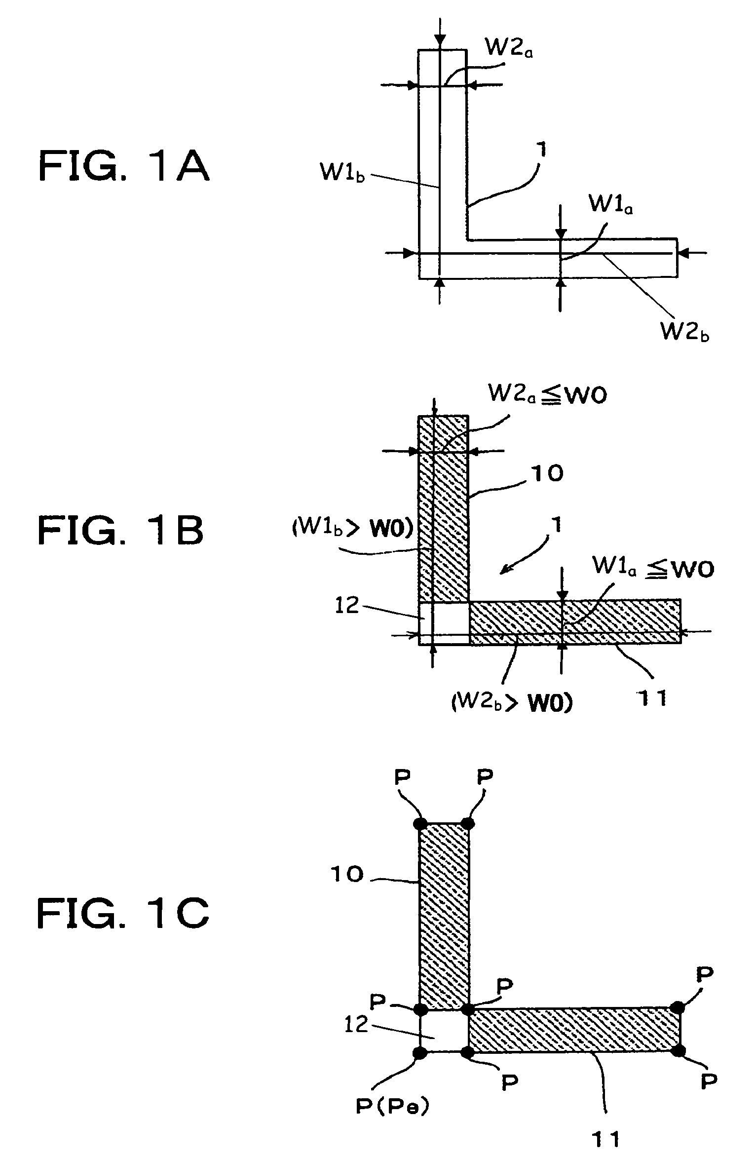
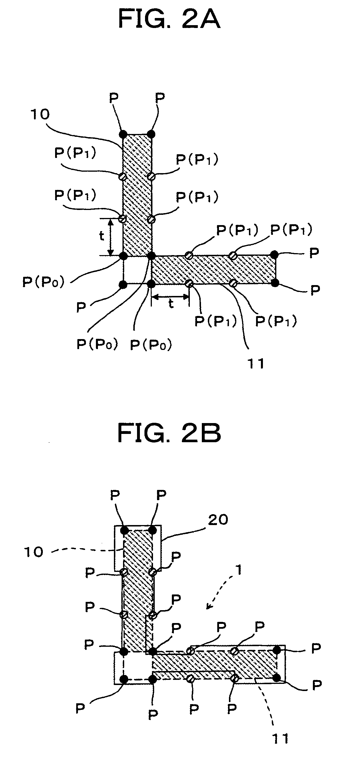
[0030]Below, an embodiment of the present invention will be explained based on the drawings. Here, an embodiment will be explained taking as an example forming an exposure mask pattern using the present invention for model-base oOPC and forming a transfer pattern of a L-shaped design pattern by lithography.

[0031]First, as shown in FIG. 1A, the different parts of the L-shaped design pattern are checked for the line widths W1 (including W1a and W1b) and W2 (including W2a and W2b) along a direction of extension (longitudinal direction). At that time, assume that the intervals between the facing sides of the design pattern 1 along the two directions serving directions of extension of the design pattern 1 (for example, the two perpendicular x- and y-directions) are detected as the line widths W1 and W2.

[0032]Next, as shown in FIG. 1B, the portions where the line widths W1 and W2 detected by the above check that are not more than the set interval WO are made the rectangular patterns 10 an...


PUM

PropertyMeasurementUnit
thicknessaaaaaaaaaa
widthsaaaaaaaaaa
optical proximity effectaaaaaaaaaa

Abstract

A method of forming an exposure mask pattern providing edge division points P at edges of a design pattern (1) by predetermined intervals and correcting edge positions for each divided edge portion, wherein, for the design pattern (1), rectangular patterns (10) and (11) are formed having pairs of facing long sides and facing short sides in the design pattern (1). The rectangular patterns (10) and (11) are formed at portions having widths W1a and W2a of the long sides in the design pattern (1) within a predetermined interval W0, so that W1a≦W0 and W2a≦W0. Next, at each of the rectangular patterns (10) and (11), new edge division points P (P1) are given along each of the facing long sides at predetermined intervals t from start points P0 sharing a short side. Due to this, the exposure mask pattern used for lithography can be simplified and the precision of formation of a transfer pattern can be improved.

Description

TECHNICAL FIELD[0001]The present invention relates to a method of forming an exposure mask pattern and an exposure mask pattern, more particularly, a method of forming an exposure mask pattern using model base proximity effect correction and an exposure mask pattern able to be obtained by the same, and a method of producing a semiconductor device.BACKGROUND ART[0002]In the process of producing a semiconductor device, ion implantation and pattern etching are performed using resist patterns as a mask.[0003]However, it is known that a resist pattern obtained by lithography and a transfer pattern formed by an etching after that suffer from variations in dimensional precision due to process conditions, the density of arrangement of patterns, underlayer conditions, and other various factors. This variation in dimensional precision becomes a factor causing short-circuits between patterns, disconnection, and other defects.[0004]Therefore, in recent years, for obtaining a transfer pattern cl...

Claims


Application Information

Patent Timeline
Patent Type & Authority Patents(United States)
IPC IPC(8): G03F1/00G03F1/24G03F1/36G03F1/68G03F7/20G06F17/50G21K5/00H01J37/00
CPCG03F1/144G03F1/36G03F1/20
Inventor OGAWA, KAZUHISAKAWAHARA, KAZUYOSHI
Owner SONY CORP
Why Eureka
Try Eureka