Method of fabricating nano-structured surface and configuration of surface enhanced light scattering probe

a technology of enhanced light scattering and nano-structured surfaces, which is applied in the direction of spectrometry/spectrophotometry/monochromators, instruments, optical radiation measurement, etc., can solve the limitation of raman spectroscopy application, the weak raman scattering signal for trace chemical detection, and the difficulty of fabricating nano-structure surfaces with reduced nano-particle dimensions, etc., to achieve the effect of enhancing surface adsorption

Inactive Publication Date: 2008-06-10
OPTOTRACE TECH
View PDF10 Cites 71 Cited by
  • Summary
  • Abstract
  • Description
  • Claims
  • Application Information

AI Technical Summary

Benefits of technology

[0010]It is therefore an object of the present invention to provide a new design of SERS and SERRS optical sensors that are suitable for portable applications. In particular, the invention is an optical sensor designed to provide ultra sensitive trace chemical detection. The sensor incorporates a nano-structured flexible noble metal surface that can be rolled onto a roller, a mechanism to protect the nano-structured surface from contamination, a method to enhance the surface adsorption by applying positive or negative voltage on the sensing surface, and a mechanism to expose a small portion of the surface for SERS or SERRS measurement.

Problems solved by technology

Historically, one of major limitations of Raman spectroscopy application is the weak Raman scattering signals for trace chemical detection.
However, the conventional technologies, for example, VLSI lithography technology, are still encountered with technical difficulties to fabricate nano-structure surfaces with reduced dimensions of the nano-particles and reduced distance among these nano-particles on the surface to achieve scattering signal enhancement.
The very limited availability of non-contaminated nano-structured noble metal surface is still a major difficulty faced by those of ordinary skill of the art in applying the technologies of Surface Enhanced Raman Scattering (SERS) and Surface Enhanced Resonant Raman Scattering (SERRS) for trace chemical detection.
Due to this limit availability, even though the detection of trace chemicals can be achieved a part-per-billion (ppb) level, the techniques of applying SERS and SERRS for detecting trace of explosives and / or other chemical materials still have very limited applications.
However, these publications do not provide an effective method to produce and package the non-contaminated nano-structured noble metal surface to achieve field applications of SERS and SERRS for trace chemical detection.
Furthermore, none of these publications provide method to fabricate nano-structured materials with well-controlled nano array that have reduced and optimized dimensions of the nano-particles and reduced and optimized distances among these nano-particles on the surface to achieve scattering signal enhancement.

Method used


Image

  • Method of fabricating nano-structured surface and configuration of surface enhanced light scattering probe
  • Method of fabricating nano-structured surface and configuration of surface enhanced light scattering probe
  • Method of fabricating nano-structured surface and configuration of surface enhanced light scattering probe

Examples


Embodiment Construction

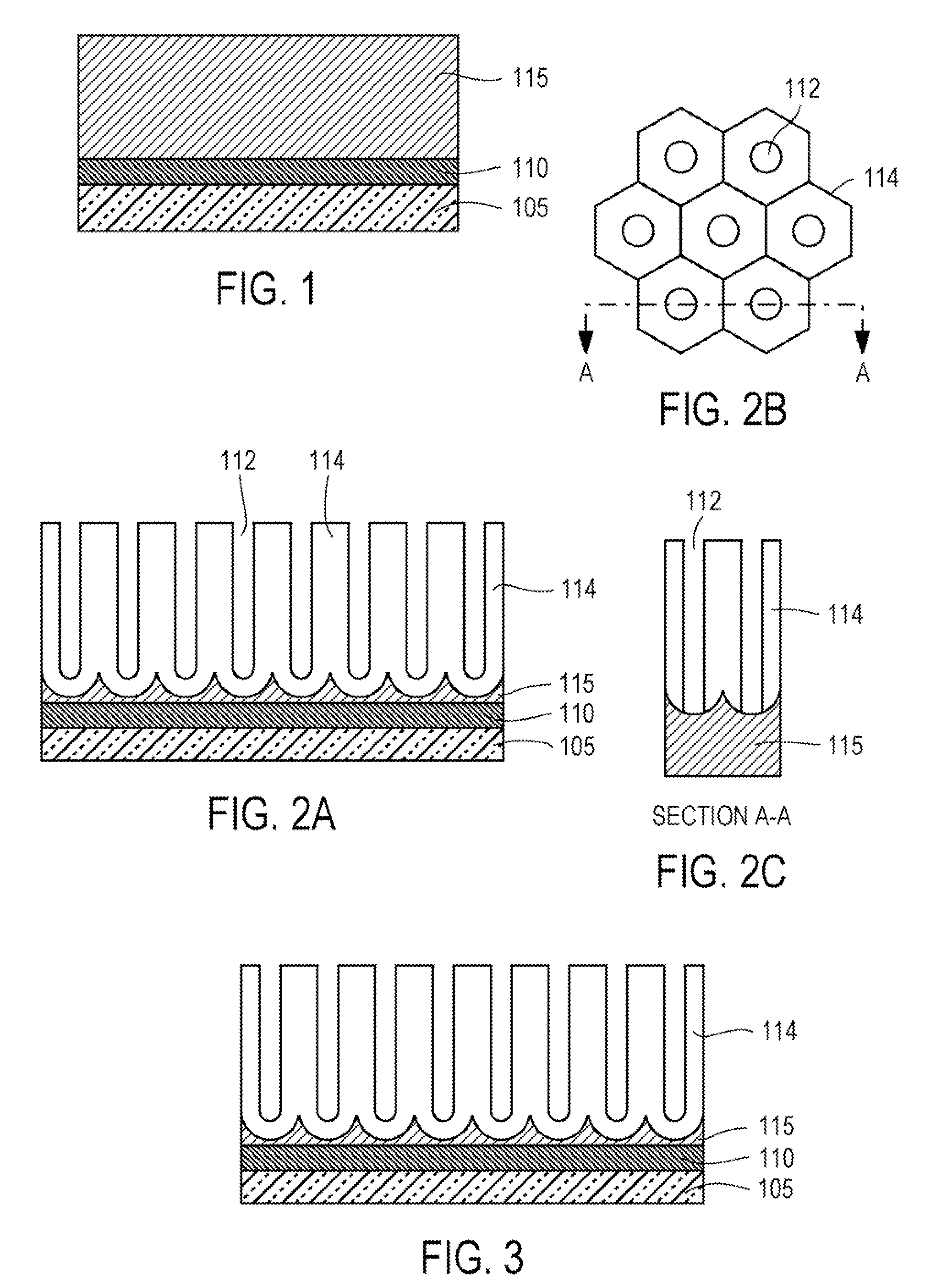
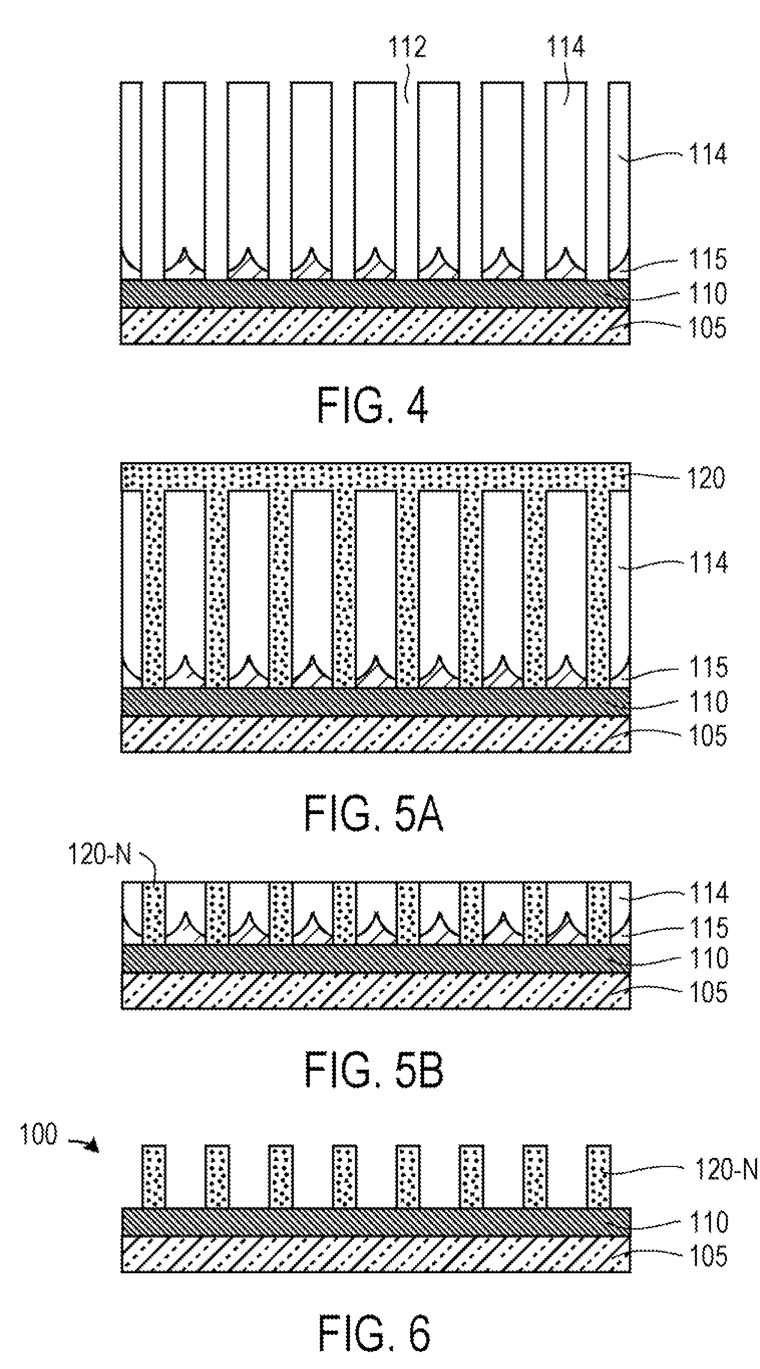
[0027]Referring to FIGS. 1 to 6 for a series of processing steps to fabricate a nano-structured noble metal surface of this invention, FIG. 1 shows a two-layer structure with n-type silicon (100) flat wafer (3-8 Ω-cm) or oxidized (30-50 nm SiO2) p-type silicon (100) flat wafers (5-10 mΩ-cm), an electrically and thermally conductive layer 110 deposited on a silicon (100) substrate 105. The thickness of the conductive layer 110, such as Ti and Ni, is optimized to provide i) best adhesion to a subsequently deposited noble metal film, such as Ag, or Au film, etc., ii) electrical conductive film to apply electrical bias to sensing surface in field application, iii) thermal conductive layer to apply lower temperature of sensing surface. The thickness of this metal film is usually controlled in the range of 100 Å-1,000 Å. Then an aluminum layer 115 with purity of 99.999% and thickness in the range of 1.0-10.0 μm is deposited on top of the conductive layer 110. Prior to anodization, silicon...


PUM

PropertyMeasurementUnit
diametersaaaaaaaaaa
heightsaaaaaaaaaa
depthsaaaaaaaaaa

Abstract

A method to fabricate an optical scattering probe and the method includes the steps of a) depositing an conductive layer on a substrate followed by depositing a noble metal layer on top of the conductive layer and then an aluminum layer on top the noble metal layer; b) anodizing the aluminum layer to form a porous aluminum oxide layer having a plurality of pores; and c) etching the plurality of pores through the aluminum oxide layer and the noble metal layer for forming a nano-hole array. In a preferred embodiment, the step of etching the plurality of pores through the aluminum oxide layer and the noble metal layer further comprising a step of widening the pores followed by removing the aluminum oxide layer for forming a plurality of noble metal column on top of the conductive layer.

Description

[0001]This application claims a Priority Date of May 27, 2003, benefited from two previously filed Provisional Applications 60 / 473,283 and 60 / 473,287 filed on May 27, 2003, and another Provisional Application 60 / 520,222 filed on Nov. 17, 2003 by at least one of a common Applicant of this patent application.BACKGROUND OF THE INVENTION[0002]1. Field of the Invention[0003]This invention relates generally to the methods and systems for detection of very small amount of trace chemicals by employing light scattering probes. More particularly, this invention relates to an improved light scattering probes and detection system based on a novel process to fabricate a sensing chip with nano-structured noble metal surface with improved configurations to detect the trace chemicals with significantly improved detection sensitivity.[0004]2. Description of the Prior Art[0005]Historically, one of major limitations of Raman spectroscopy application is the weak Raman scattering signals for trace chemi...

Claims


Application Information

Patent Timeline
Patent Type & Authority Patents(United States)
IPC IPC(8): G01N21/03B32B3/02B32B7/12G01J3/44G01N21/65G01N33/558H01J9/04
CPCG01J3/44G01N21/658Y10T428/28Y10T428/218
Inventor WANG, HONGLIU, ZHIMIN
Owner OPTOTRACE TECH
Why Eureka
Try Eureka