Standby leakage current reduction circuit and semiconductor memory device comprising the standby leakage current reduction circuit

a technology reduction circuit, which is applied in the direction of information storage, static storage, digital storage, etc., can solve the problems of inability to account for conventional semiconductor memory devices, increase and affect certain operating characteristics of memory cells, etc., to reduce excess power consumption and reduce the amount of standby leakage current

Active Publication Date: 2008-07-08
SAMSUNG ELECTRONICS CO LTD
View PDF8 Cites 25 Cited by
  • Summary
  • Abstract
  • Description
  • Claims
  • Application Information

AI Technical Summary

Benefits of technology

[0029]Accordingly, embodiments of the invention provide a standby leakage current reduction circuit and a semiconductor memory device comprising the standby leakage current reduction circuit, wherein the standby leakage current reduction circuit is adapted to reduce standby leakage current that may be caused by process scatter, (e.g., variations in process pressure, voltage or temperature (PVT)), and is further adapted to reduce excess power consumption caused by standby leakage current.

Problems solved by technology

When a high level power source voltage HVCC (i.e., a power source voltage VCC having a relatively high voltage level) is applied in the semiconductor memory device, the amount of standby leakage current may increase.
One shortcoming of this method of increasing the threshold voltage Vth of a MOS transistor in a memory cell is that certain operating characteristics of the memory cell may become impaired when a relatively low external power source voltage LVCC is applied in the semiconductor memory device.
However, a limitation in conventional semiconductor memory devices is that conventional semiconductor memory devices do not account for process variation or temperature variation when reducing standby leakage current.
Conventional semiconductor memory devices suffer from problems such as data loss and the consumption of excess power as a result of standby leakage current caused by variations in temperature, external power source voltage, and fabrication process (hereafter “process scatter”).

Method used


Image

  • Standby leakage current reduction circuit and semiconductor memory device comprising the standby leakage current reduction circuit
  • Standby leakage current reduction circuit and semiconductor memory device comprising the standby leakage current reduction circuit
  • Standby leakage current reduction circuit and semiconductor memory device comprising the standby leakage current reduction circuit

Examples


Embodiment Construction

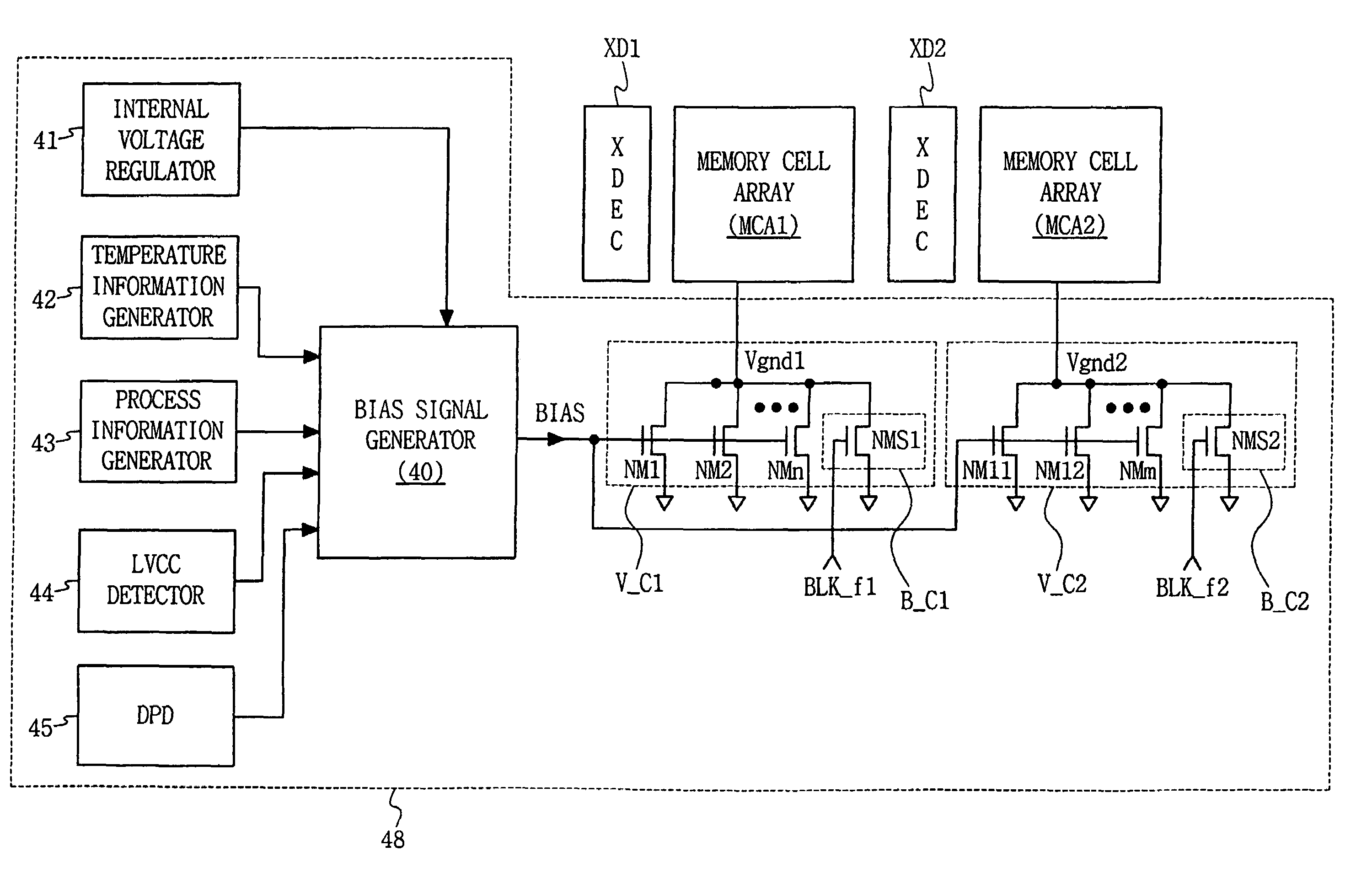
[0050]FIG. 4 schematically illustrates a semiconductor memory device in accordance with an embodiment of the invention that comprises a standby leakage current reduction circuit in accordance with an embodiment of the invention.

[0051]Referring to FIG. 4, a bias signal generator 40 operates in accordance with a voltage controlled by and received from an internal voltage regulator 41; receives signals output from a temperature information generator 42, a process information generator 43, an LVCC detector 44, and a deep power down setting unit 45; and generates and outputs a bias signal BIAS.

[0052]In addition, first ground voltage controller V_C1 receives bias signal BIAS and controls the level of the voltage apparent on first virtual ground terminal Vgnd1 of memory cells of first memory cell array MCA1. Similarly, second ground voltage controller V_C2 receives bias signal BIAS and controls the level of the voltage apparent on second virtual ground terminal Vgnd2 of memory cells of sec...


PUM


Abstract

Embodiments of the invention provide a standby leakage current reduction circuit and a semiconductor memory device comprising the standby leakage current reduction circuit. The invention provides a circuit adapted to reduce standby leakage current in a semiconductor memory device comprising memory cells. The circuit comprises a bias signal generator adapted to generate a bias signal, wherein a voltage level of the bias signal is set in accordance with a result of a standby leakage current test. The circuit further comprises a ground voltage controller adapted to receive the bias signal from the bias signal generator and to control a level of a voltage apparent on a virtual ground terminal in response to the bias signal while the semiconductor memory device is in a standby mode.

Description

BACKGROUND[0001]1. Field of the Invention[0002]Embodiments of the invention relate to a semiconductor memory device. In particular, embodiments of the invention relate to a standby leakage current reduction circuit and a semiconductor memory device comprising the standby leakage current reduction circuit.[0003]This application claims priority to Korean Patent Application 10-2005-0131194, filed on Dec. 28, 2005, the subject matter of which is hereby incorporated by reference in its entirety.[0004]2. Description of Related Art[0005]Generally, standby current in a semiconductor memory device may be current that leaks from a semiconductor memory device while the semiconductor memory device is in a standby mode. Standby current may also be referred to herein as standby leakage current.[0006]An active mode of a semiconductor memory device may be a mode in which peripheral circuits of the semiconductor memory device operate to store data in memory cells of the semiconductor memory device o...

Claims


Application Information

Patent Timeline
Patent Type & Authority Patents(United States)
IPC IPC(8): G11C5/14
CPCG11C5/148G11C11/413G11C29/021G11C29/028G11C29/02G11C11/41G11C2029/5006
Inventor LEE, YOUNG-DAE
Owner SAMSUNG ELECTRONICS CO LTD
Why Eureka
Try Eureka