Method for forming an integrated circuit

a technology of integrated circuits and integrated circuits, applied in the field of forming nmos transistors, can solve the problems of high dislocation defect density, high tensile strain, cost and complexity of the sige integration scheme,

Active Publication Date: 2008-07-22
TAHOE RES LTD
View PDF15 Cites 140 Cited by
  • Summary
  • Abstract
  • Description
  • Claims
  • Application Information

AI Technical Summary

Problems solved by technology

Limitations with respect to this approach include: (1) an inability to generate high levels of tensile strain, (2) high dislocation defect densities, (3) the cost and complexity of the SiGe integration scheme, and (4) the production of an offsetting decrease in hole mobility that can degrade p-MOS transistor performance.

Method used


Image

  • Method for forming an integrated circuit
  • Method for forming an integrated circuit
  • Method for forming an integrated circuit

Examples


Embodiment Construction

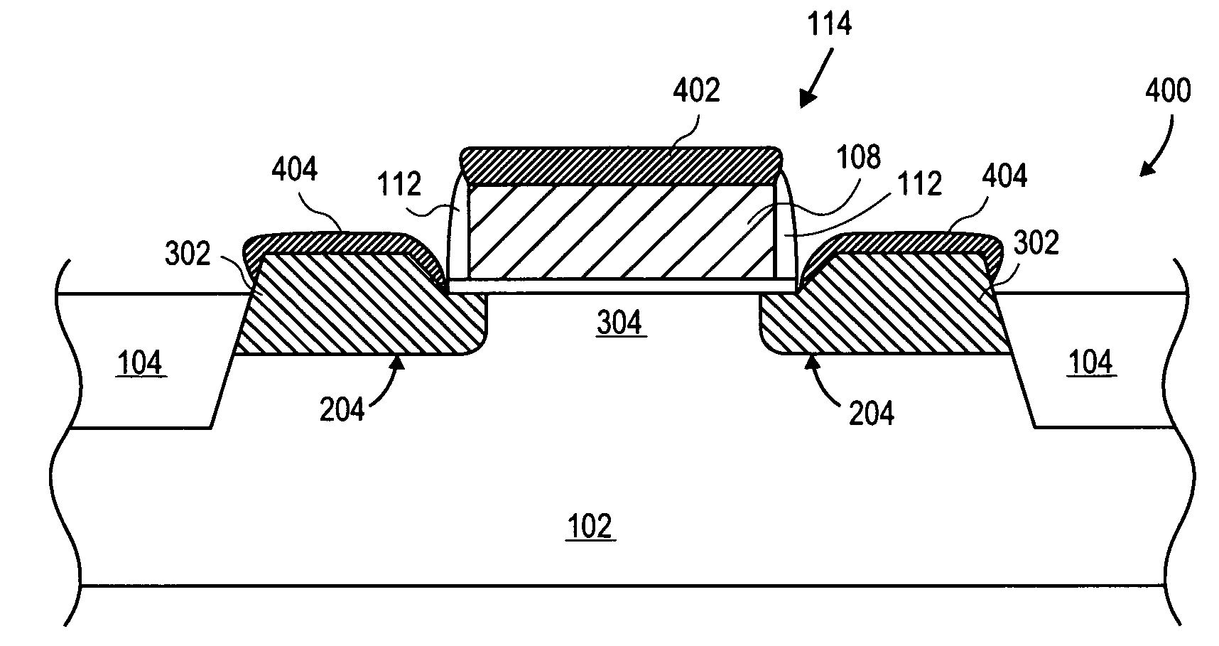
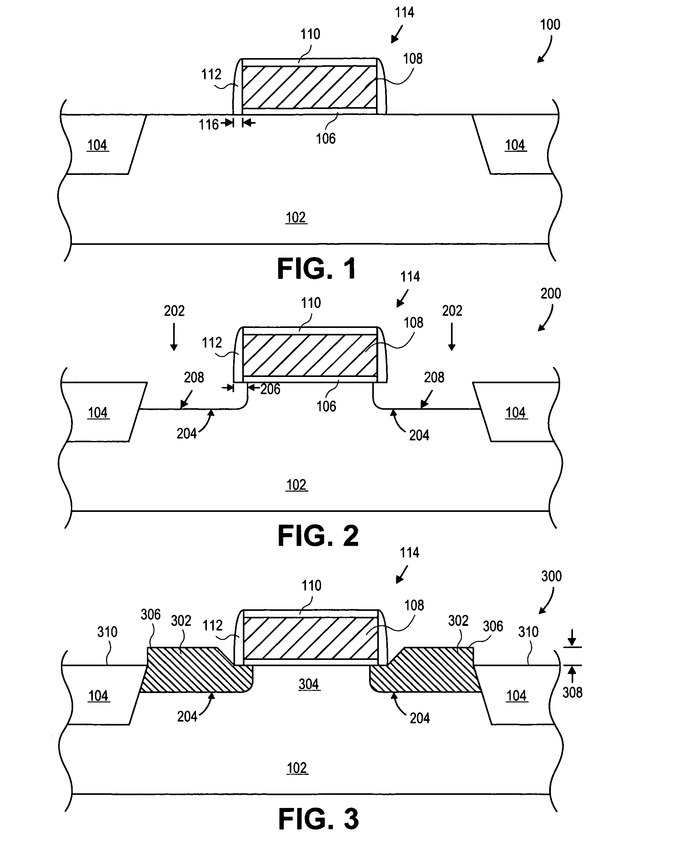
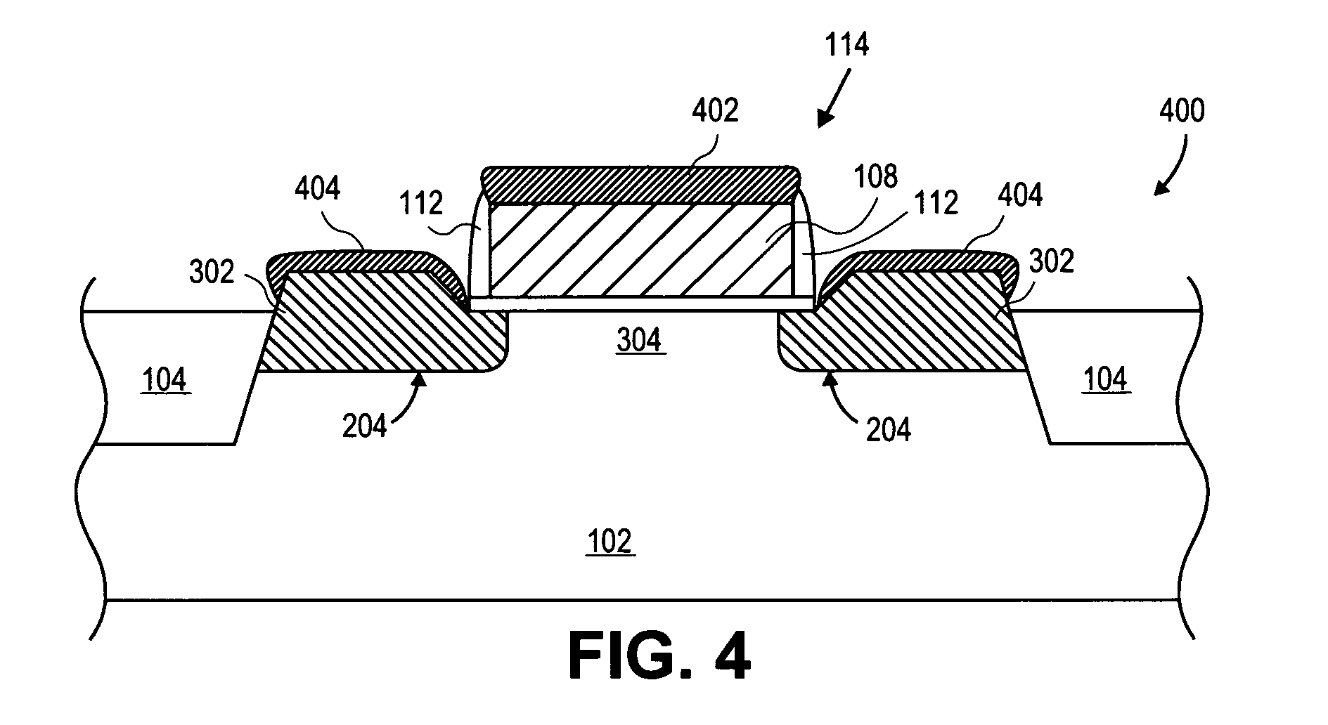
[0013]In the following detailed description, an n-MOS transistor and its method of formation are disclosed. Reference is made to the accompanying drawings, which form a part hereof, and within which are shown by way of illustration specific embodiments by which the present invention may be practiced. It is to be understood that other embodiments may be utilized and structural changes may be made without departing from the scope and spirit of the present invention.

[0014]In one embodiment, recesses are etched in a semiconductor material (such as silicon), and source / drain regions are epitaxially deposited into the recesses. The source / drain regions can include carbon (C), phosphorus (P), or combinations thereof that have been substitutionally incorporated into the epitaxial silicon crystal lattice during the deposition process.

[0015]The carbon source for the epitaxial deposition can be a carbon-containing precursor, such as monomethyl silane, and the epitaxial deposition chamber set-p...


PUM

PropertyMeasurementUnit
depthaaaaaaaaaa
thicknessaaaaaaaaaa
pressureaaaaaaaaaa

Abstract

A method is described for manufacturing an n-MOS semiconductor transistor. Recesses are formed in a semiconductor substrate adjacent a gate electrode structure. Silicon is embedded in the recesses via a selective epitaxial growth process. The epitaxial silicon is in-situ alloyed with substitutional carbon and in-situ doped with phosphorus. The silicon-carbon alloy generates a uniaxial tensile strain in the channel region between the source and drain, thereby increasing electron channel mobility and the transistor's drive current. The silicon-carbon alloy decreases external resistances by reducing contact resistance between source / drain and silicide regions and by reducing phosphorous diffusivity, thereby permitting closer placement of the transistor's source / drain and channel regions.

Description

[0001]This is a Divisional application of Ser. No.: 10 / 993,865 filed Nov. 18, 2004, now abandoned.FIELD OF THE INVENTION[0002]Embodiments of the present invention relate generally to semiconductor processing and more specifically to methods for forming n-MOS transistors.BACKGROUND OF THE INVENTION[0003]In silicon (Si) based microelectronics, a key parameter in assessing device performance is the current delivered at a given design voltage. This parameter is commonly referred to as transistor drive current or saturation current (IDsat). Drive current is affected by factors that include the transistor's channel mobility and external resistance.[0004]Channel mobility refers to the mobility of carriers (i.e. holes and electrons) in the transistor's channel region. Increased carrier mobility translates directly into increased drive current at a given design voltage and gate length. Carrier mobility can be increased by straining the channel region's silicon lattice. For n-MOS devices, car...

Claims


Application Information

Patent Timeline
Patent Type & Authority Patents(United States)
IPC IPC(8): H01L29/76H01L29/94H01L31/062H01L31/113
CPCH01L29/665H01L29/7834H01L29/66636
Inventor MURTHY, ANAND S.GLASS, GLENN A.WESTMEYER, ANDREW N.HATTENDORF, MICHAEL L.GHANI, TAHIR
Owner TAHOE RES LTD
Why Eureka
Try Eureka