Oxide semiconductor device and method of manufacturing the same and active matrix substrate

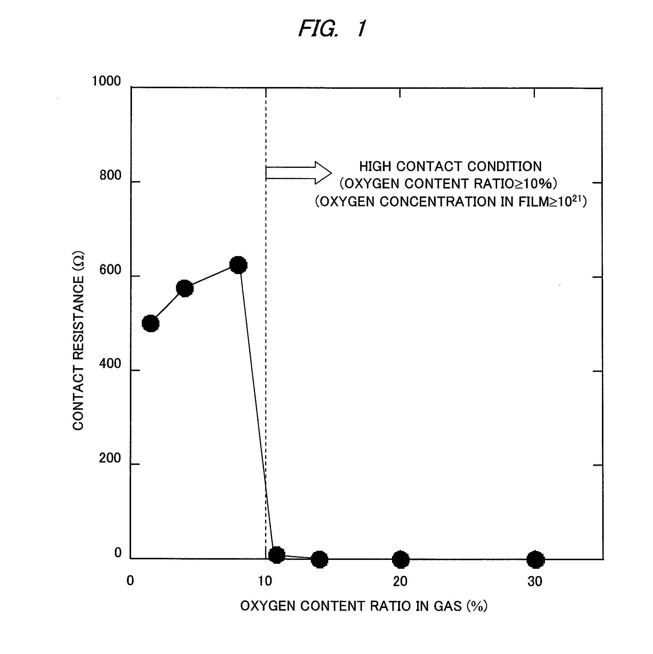
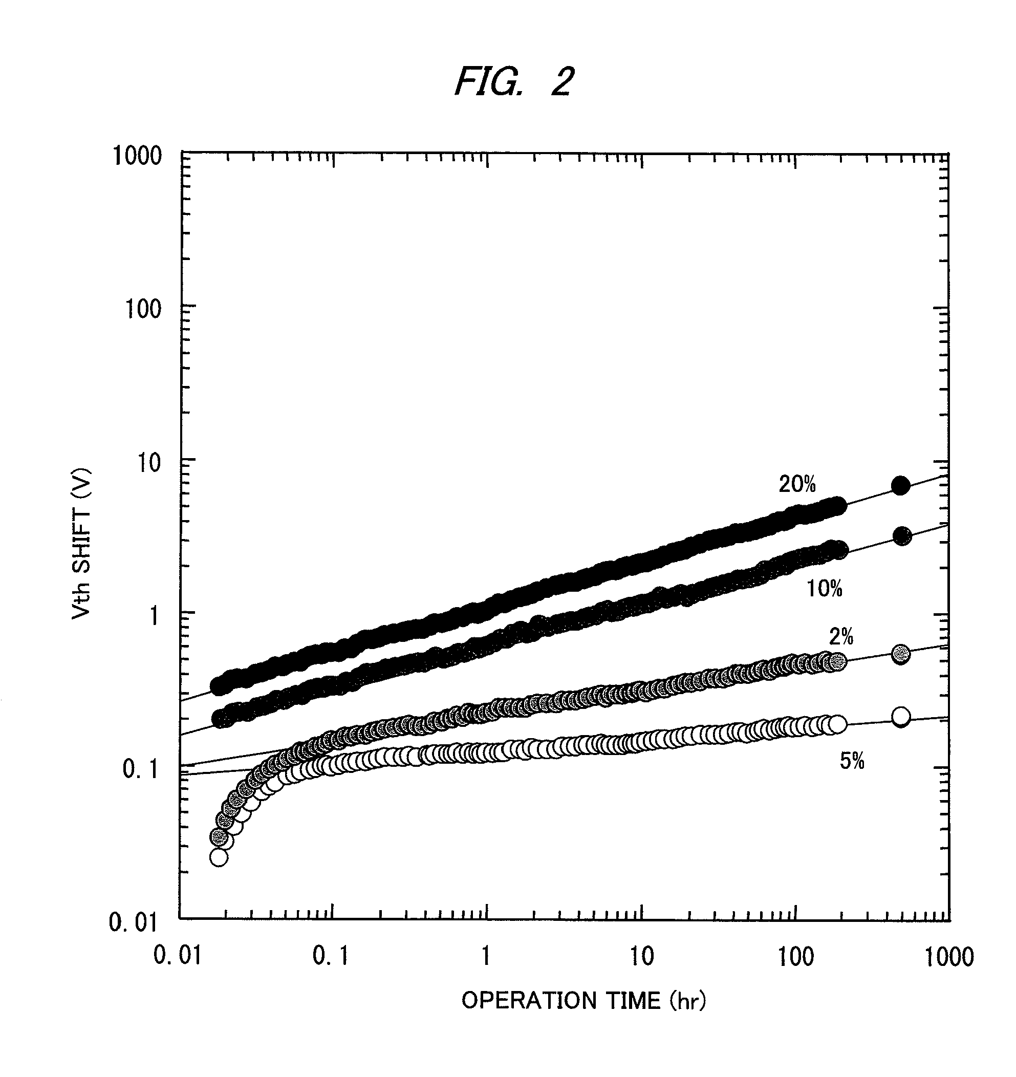
a technology of active matrix substrate and semiconductor, which is applied in the direction of semiconductor devices, electrical devices, transistors, etc., can solve the problems of difficult to use a—si for a thin-film transistor for organic el, oxide semiconductor are not fully used, and good contact properties cannot be obtained, so as to achieve significant improvement of threshold potential shift, high oxygen content ratio, and large threshold potential shift

Inactive Publication Date: 2010-06-10
HITACHI LTD
View PDF9 Cites 92 Cited by
  • Summary
  • Abstract
  • Description
  • Claims
  • Application Information

AI Technical Summary

Benefits of technology

[0013]As illustrated in FIGS. 1 and 2, in the condition of the high oxygen content ratio, although a good contact property is shown, the threshold potential shift is large. On the other hand, in the region of the low oxygen content ratio, although a good threshold potential shift is shown, the contact property is bad, and therefore, it is difficult to balance these two competing issues. Accordingly, FIGS. 4 and 5 illustrate states of the contact resistance and the threshold potential shift when applying the present invention of the present application to a multilayered structure in which, in an oxide semiconductor layer having a total thickness of 25 nm, an oxygen content ratio in an introduced gas is set to be 4% upon depositing the oxide semiconductor layer for a thickness of 20 nm in the vicinity of the gate insulating film, and the oxygen content ratio upon depositing the oxide semiconductor layer is changed for a thickness of 5 nm from a portion contacting with the source / drain electrode. For comparison, results of a conventional structure are also illustrated. Compared with the case of using a single oxide semiconductor channel layer having an oxygen content ratio of 20%, the threshold potential shift is significantly improved in the case of the multilayered structure as keeping a good contact resistance to the source / drain electrode. For comparison, in a manner opposite to the method of the present invention, a measurement is performed on an oxide semiconductor layer having the oxygen content ratio of 4% upon depositing the oxide semiconductor layer for the thickness of 5 nm of the layer contacting with the metal and an oxide semiconductor layer having the oxygen content ratio of 20% upon depositing the oxide semiconductor layer for the thickness of 20 nm of the main channel layer. A result of this measurement is different from that of the method of the present invention, and the result showed a very high contact resistance of almost 1 kΩ and the threshold potential shift could not be measured. Also from this point, the method of the present invention clearly improves the contact property between the electrode metal and the oxide semiconductor layer.

Problems solved by technology

More particularly, since application as a current-driving device has been required for an organic EL display expected as an spontaneous light emission and high-definition display in recent years, large reliabilities in its durability and suppression of its threshold potential shift are required.
For example, since a threshold potential shift of a—Si that has been conventionally and mainly used for a pixel switching of a liquid crystal display is largely over about 2 V which is easily controlled by a correction circuit, it is considered to be difficult to use the a—Si for a thin-film transistor for organic EL.
However, in an oxide semiconductor to which studies on an interface of semiconductor / electrode have not been developed compared with that of a Si semiconductor, there is an issue that good contact property cannot be obtained because of control of the interface of the oxide semiconductor and the electrode or differences in work function between the oxide semiconductor and metal materials, and properties included in the oxide semiconductor are not fully used. FIGS. 1 and 2 are diagrams illustrating a relation of a contact resistance and an oxygen content ratio with respect to argon gas and a relation of a threshold potential shift and the oxygen content ratio, respectively, when an oxide semiconductor channel layer is formed of IGZO by sputtering deposition.
On the other hand, when the oxygen content ratio is 5% or lower, while the threshold potential shift is good, the contact resistance is high, and therefore, it is difficult to balance these competing issues.
However, since the oxide semiconductor layer being the channel layer is formed of a complex oxide mainly made of indium or zinc oxide, a composition of the layer is changed at an interface contacting to these transparent conductive film materials, and there are possibilities of affecting a semiconductor property and causing a property change by energization, and therefore, the method is not necessarily good.
However, accurate oxygen concentration control is difficult because of difficulty of plasma control depending on an inside state of a vacuum chamber, and the exposure cannot be treated in a state before forming the oxide semiconductor layer because it is a surface process.
That is, the treatment is possible if the transistor has a top-contact type thin-film transistor structure, and the treatment is impossible if the transistor has a bottom-contact type thin-film transistor structure.

Method used


Image

  • Oxide semiconductor device and method of manufacturing the same and active matrix substrate
  • Oxide semiconductor device and method of manufacturing the same and active matrix substrate
  • Oxide semiconductor device and method of manufacturing the same and active matrix substrate

Examples


first embodiment

[0037]A structure of a thin-film transistor for an image device according to a first embodiment of the present invention, a method of manufacturing the same, and a method of employing the device and method will be described with reference to FIGS. 7A to 10C. FIGS. 7A to 7E illustrate cross-sectional views of a bottom-gate top-contact thin-film transistor and also flow diagrams illustrating one example of a method of manufacturing the transistor. FIGS. 8 and 9 illustrate a simple configuration of an active-matrix circuit for employing the transistor to a device and a schematic view of the active-matrix circuit, respectively. FIG. 10 is a cross-sectional view illustrating a structure of a thin-film transistor having a structure other than the bottom-gate top-contact structure.

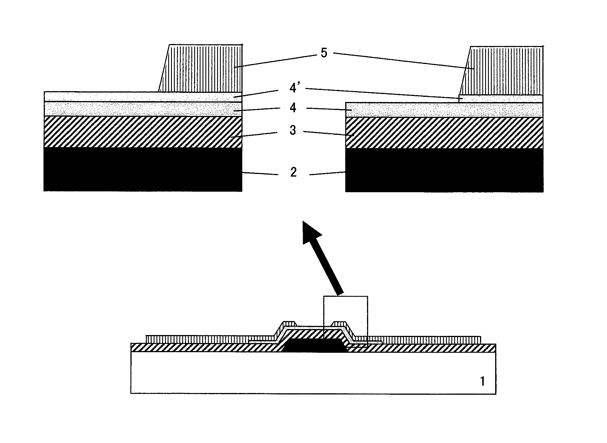
[0038]First, there is prepared a supporting substrate 1 such as, for example, a glass substrate, a quartz substrate, a sapphire substrate, a resin substrate, or a film. Next, there is formed a stacked film of met...

second embodiment

[0044]A structure of an oxide semiconductor thin film memory according to a second embodiment of the present invention and a method of manufacturing the same will be described with reference to FIGS. 11A to 16. FIGS. 11A-11E and 12 illustrate cross-sectional views of an oxide semiconductor thin film memory using a bottom-gate top-contact thin-film transistor according to the present invention and flow diagrams illustrating one example of a manufacturing process of the memory. FIG. 13A illustrates a memory structure including a capacitor on the drain side and FIG. 14A illustrates a memory configuration for performing a memory operation by a change of a gate capacitance, and FIG. 13B and FIG. 14B illustrate cross-sectional views of these memory devices, respectively. FIGS. 15A and 15B are cross-sectional views each illustrating one example of integrating a display-driving transistor using the bottom-gate top-contact thin-film transistor according to the method of the present invention...

third embodiment

[0050]A structure of a touch panel using an oxide semiconductor thin-film transistor according to a third embodiment of the present invention and a method of manufacturing the same will be described with reference to FIGS. 17A-17D and 18. FIGS. 17A-17D are cross-sectional views of an oxide semiconductor touch panel (touch sensor) according to the present invention and flow diagrams illustrating one example of a manufacturing process of the oxide semiconductor touch panel. FIG. 18 is a cross-sectional view illustrating one example in which the oxide semiconductor touch panel and the oxide semiconductor transistor according to the present invention are integrated as a back-emission type organic EL display.

[0051]Although a basic structure of the touch panel according to the present invention is almost the same with that of the oxide semiconductor thin-film transistor array described in the second embodiment, no surface unevenness is desirable in a surface of the structure of the touch ...


PUM


Abstract

A phenomenon of change of a contact resistance between an oxide semiconductor and a metal depending on an oxygen content ratio in introduced gas upon depositing an oxide semiconductor film made of indium gallium zinc oxide, zinc tin oxide, or others in an oxide semiconductor thin-film transistor. A contact layer is formed with an oxygen content ratio of 10% or higher in a region from a surface, where the metal and the oxide semiconductor are contacted, down to at least 3 nm deep in depth direction, and a region to be a main channel layer is further formed with an oxygen content ratio of 10% or lower, so that a multilayered structure is formed, and both of ohmic characteristics to the electrode metal and reliability such as the suppression of threshold potential shift are achieved.

Description

CROSS-REFERENCE TO RELATED APPLICATION[0001]The present application claims priority from Japanese Patent Application No. JP 2008-312814 filed on Dec. 9, 2008, the content of which is hereby incorporated by reference into this application.TECHNICAL FIELD OF THE INVENTION[0002]The present invention relates to an oxide semiconductor device and a technique of manufacturing the same.BACKGROUND OF THE INVENTION[0003]In recent years, a display device has been flat-surface display device from a display using a cathode-ray tube toward a flat-surface display device called flat panel display (FPD) such as a liquid crystal panel and a plasma display. In the liquid crystal panel, as an element relating to pixel switching by liquid crystals, a thin-film transistor made of a—Si (amorphous silicon) or poly-silicon is used for a switching element. Recently, an FPD using organic Electro-Luminescence (EL) has been expected aiming for further larger area size and flexibility. However, since the organic...

Claims


Application Information

Patent Timeline
Patent Type & Authority Applications(United States)
IPC IPC(8): H01L29/24H01L21/36
CPCH01L21/02554H01L21/02565H01L21/02617H01L21/28291H01L27/10873H01L51/5206H01L27/11206H01L27/1225H01L27/3276H01L29/7869H01L27/112H01L29/40111H10B12/05H10B20/20H10B20/00H10K59/1213H10K50/81
Inventor UCHIYAMA, HIROYUKIKAWAMURA, TETSUFUMIWAKANA, HIRONORI
Owner HITACHI LTD
Why Eureka
Try Eureka