Conductive pattern forming method and conductive pattern forming system

a technology of conductive polymer and conductive pattern, which is applied in the direction of superimposed coating process, liquid/solution decomposition chemical coating, resistive material coating, etc., can solve the problems of low electrical conductivity (conductivity), performance (adhesion) with resin substrate and flexibility, and electrical performance becomes an issue, so as to increase the content ratio of metal microparticles, the effect of favorable electrical performan

Inactive Publication Date: 2013-05-23
FUJIFILM CORP
View PDF1 Cites 9 Cited by
  • Summary
  • Abstract
  • Description
  • Claims
  • Application Information

AI Technical Summary

Benefits of technology

[0010]According to the present invention, since a conductive pattern having a graded composition structure in which a content ratio of a conductive polymer decreases while a content ratio of metal microparticles increases from a base material is formed with respect to a thickness direction, adhesion with the base material is secured at a bonding portion between the base material and the conductive pattern due to the high content ratio of the conductive polymer and, at the same time, favorable electrical performance is produced by increasing the content ratio of the metal microparticles.

Problems solved by technology

However, with the functional fluid prepared by dispersing metal particles in a conductive polymer which is used in the method of manufacturing an organic EL display device disclosed in Japanese Patent Application Publication No. 2004-302392, a bonding performance (adhesion) with a resin substrate and flexibility become an issue if a content of metal particles is increased in order to improve electrical performance.
On the other hand, reducing the content of metal particles results in lower electrical conductivity (conductivity) and electrical performance becomes an issue.

Method used


Image

  • Conductive pattern forming method and conductive pattern forming system
  • Conductive pattern forming method and conductive pattern forming system
  • Conductive pattern forming method and conductive pattern forming system

Examples


first embodiment

Overview of Conductive Pattern Forming Method (System)

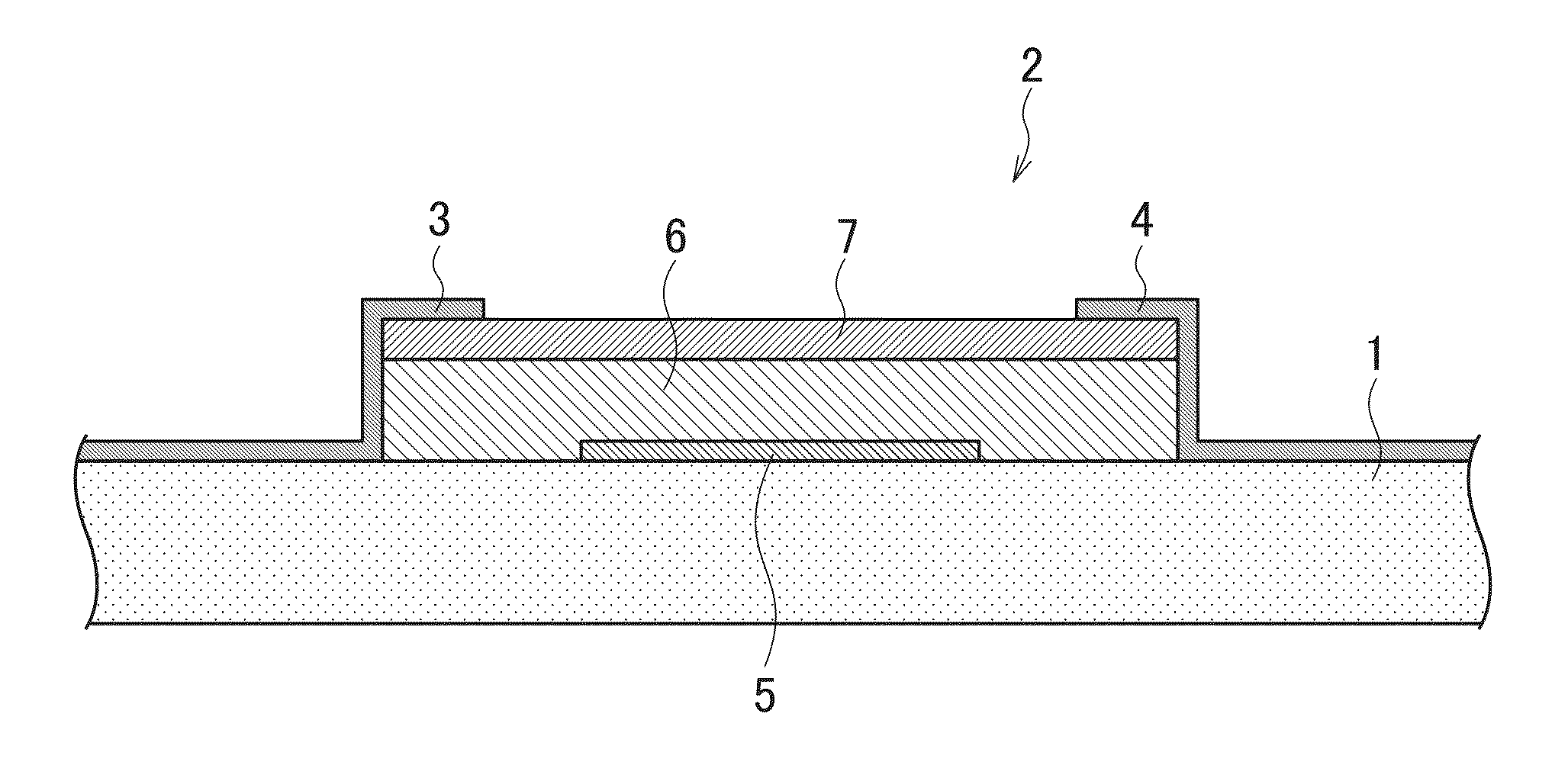
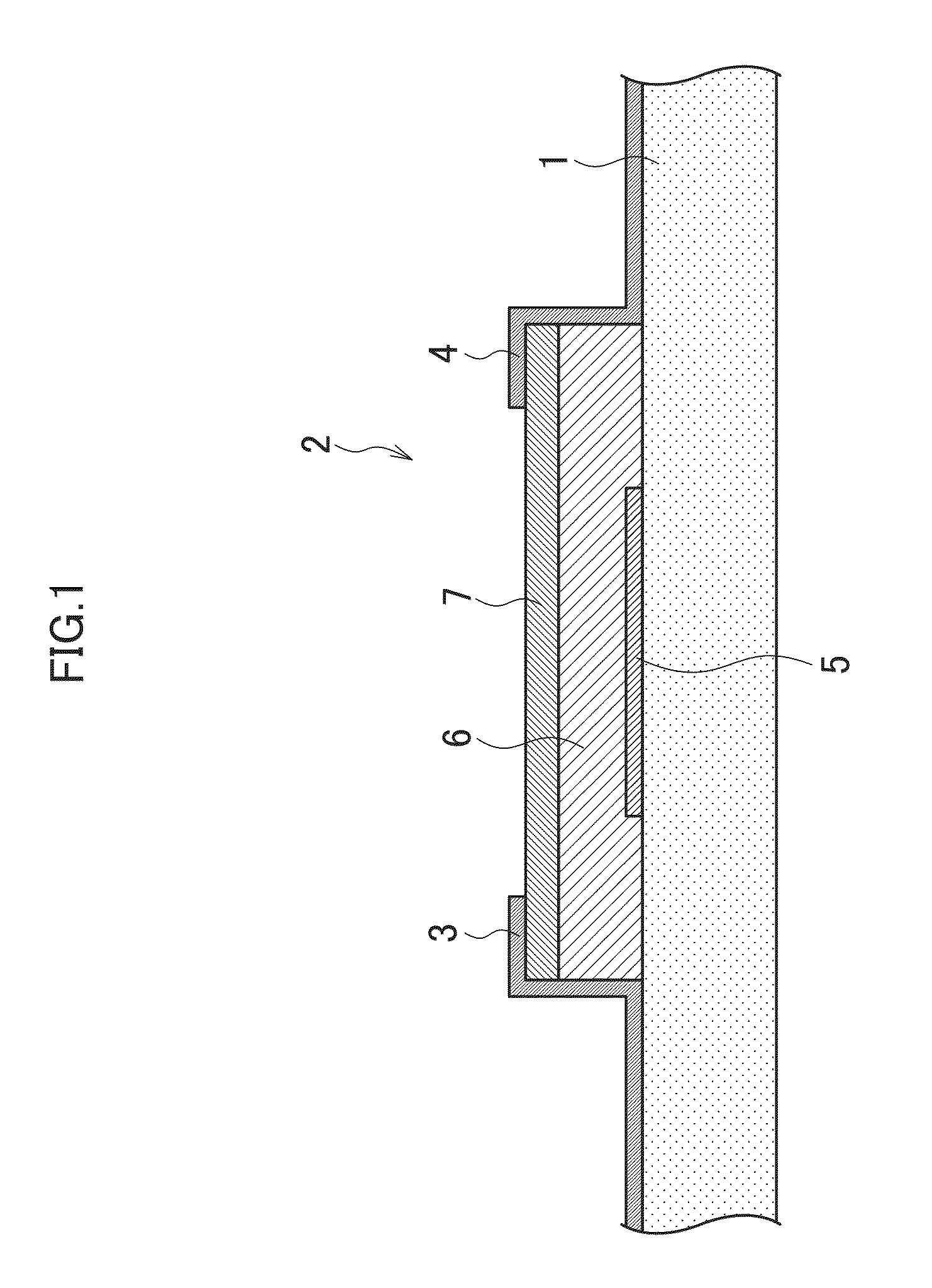
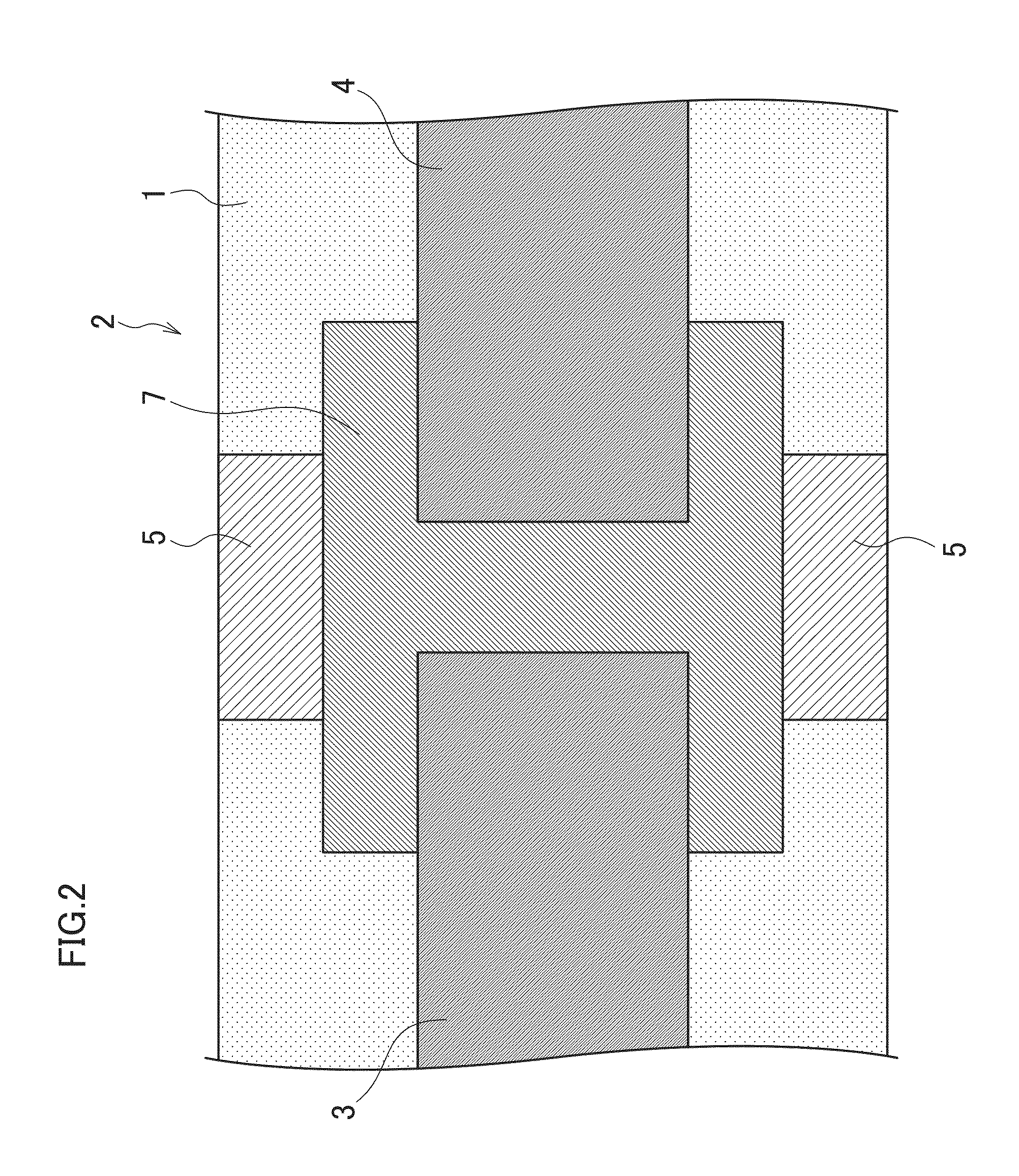
[0048]FIG. 1 is an explanatory diagram of a conductive pattern forming method (system) according to a first embodiment of the present invention and is a sectional view showing a schematic structure of electrical wirings (electrodes or electrode wirings) 3, 4, and 5 of an organic TFT (Thin Film Transistor) 2 formed on a flexible film (flexible base material) 1.

[0049]In the first embodiment described below, a description will be given on conductive pattern formation according to an ink-mixing method in which a conductive polymer and metal nanoparticles are mixed in advance at a predetermined content ratio and a plurality of functional fluids with different content ratios of the conductive polymer and the metal nanoparticles are used.

[0050]Note that in the present specification, the “flexible film 1” and the “organic TFT 2” may also be collectively referred to as a “base material” without distinction between the “flexible film 1” an...

second embodiment

[0231]Next, a conductive pattern forming method (system) according to a second embodiment of the present invention will be described.

[0232](Description of Conductive Pattern Forming System (Device))

[0233]FIG. 17 is a general configuration diagram of a conductive pattern forming system according to the second embodiment of the present invention. Moreover, in FIG. 17, portions that are same as or similar to those in FIG. 4 are denoted by same reference numerals and descriptions thereof will be omitted.

[0234]A pattern forming system 110 shown in FIG. 17 includes an ink-jet head 50-11 that discharges a functional fluid containing a conductive polymer (a conductive polymer fluid) and an ink-jet head 50-12 that discharges a functional fluid containing metal nanoparticles (a metal nanoparticle fluid) in place of the ink-jet heads 50-1, 50-2, 50-3, 50-4, and 50-5 which discharge functional fluids of the conductive pattern forming system 10 illustrated in FIG. 4.

[0235]A draw-mixing method is...

specific application examples

[0296]Next, application examples of a wiring structure formed using the conductive pattern forming method (system) presented above will be described. FIG. 22 is a sectional perspective view of a touch panel 200 formed using the conductive pattern forming method described above.

[0297]For the touch panel 200 shown in FIG. 22, colorless and transparent indium tin oxide (ITO) is used as a material of metal nanoparticles. In other words, the conductive pattern forming method shown in the present example is applied to a transparent electrode film 204 of an upper conductive layer 202 and a transparent electrode film 208 of a lower electrode layer 206.

[0298]A member denoted by reference numeral 210 is a front panel and a member denoted by reference numeral 212 is a base substrate. A detailed description of a structure and a description of functions of the touch panel 200 will be omitted.

[0299]According to the conductive pattern forming method and the conductive pattern forming system config...


PUM

PropertyMeasurementUnit
boiling pointaaaaaaaaaa

Abstract

According to a mode of the present invention, since a conductive pattern having a graded composition structure in which a content ratio of a conductive polymer decreases while a content ratio of metal microparticles increases from a base material is formed with respect to a thickness direction, adhesion with the base material is secured at a bonding portion between the base material and the conductive pattern due to the high content ratio of the conductive polymer and, at the same time, favorable electrical performance is produced by increasing the content ratio of the metal microparticles.

Description

BACKGROUND OF THE INVENTION[0001]1. Field of the Invention[0002]The present invention relates to a conductive pattern forming method and a conductive pattern forming system and, more specifically, to wiring formation and conductive film formation on a flexible material such as organic resin using an ink-jet method.[0003]2. Description of the Related Art[0004]In recent years, proposals have been made in regards to wiring drawing according to printable electronics using printing technology. Japanese Patent Application Publication No. 2004-302392 discloses a method of manufacturing an organic EL display device in which a functional fluid prepared by dispersing metal particles in a conductive polymer is applied to a flexible and irreversible resin substrate (a flexible substrate) in order to form wirings such as a power line, a signal line, a scanning line, active elements such as a transistor, and light-emitting pixels.[0005]In addition, Japanese Patent Application Publication No. 6-93...

Claims


Application Information

Patent Timeline
Patent Type & Authority Applications(United States)
IPC IPC(8): H05K3/12
CPCH05K3/125H01L51/0022H01L51/102H01L51/0545H01L51/0037H10K71/611H10K85/1135H10K10/82H10K10/466
Inventor KATSUMURA, MANABU
Owner FUJIFILM CORP
Why Eureka
Try Eureka