Device and method for organic vapor jet deposition

a technology of organic vapor jet and deposition chamber, which is applied in the direction of steam generation using steam absorption, combustion air/fuel air treatment, machines/engines, etc., can solve the problems of large amount of evaporant on the cold walls of the deposition chamber, difficult control of film thickness uniformity and dopant concentration over large areas, and contaminating system and substrate with particulates

Active Publication Date: 2008-07-29
THE TRUSTEES FOR PRINCETON UNIV
View PDF26 Cites 72 Cited by
  • Summary
  • Abstract
  • Description
  • Claims
  • Application Information

AI Technical Summary

Benefits of technology

[0011]It is an object of the present invention to provide a device for the patterned deposition of organic materials onto substrates that utilizes the vapor transport mechanisms of organi...

Problems solved by technology

However, control of film thickness uniformity and dopant concentrations over large areas needed for manufactured products can be difficult when using vacuum evaporation (see S. Wolf and R. N. Tauber, Silicon Processing for the VLSI Era (Lattice, 1986)).
In addition, a considerable fraction of the evaporant coats the cold walls of the deposition chamber.
Over time, inefficient use of materials results in a thick coating which can flake off, leading to particulate contamination of the system and substrate.
The potential throughput for vacuum evaporated organic thin film devices is low, resulting in high production co...

Method used


Image

  • Device and method for organic vapor jet deposition
  • Device and method for organic vapor jet deposition
  • Device and method for organic vapor jet deposition

Examples


example 1

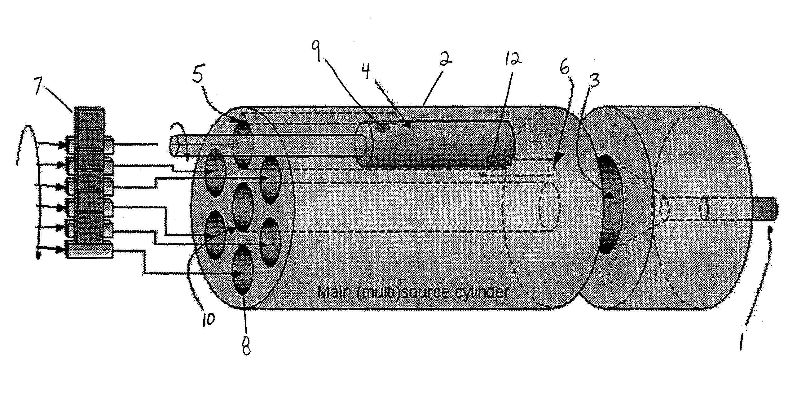
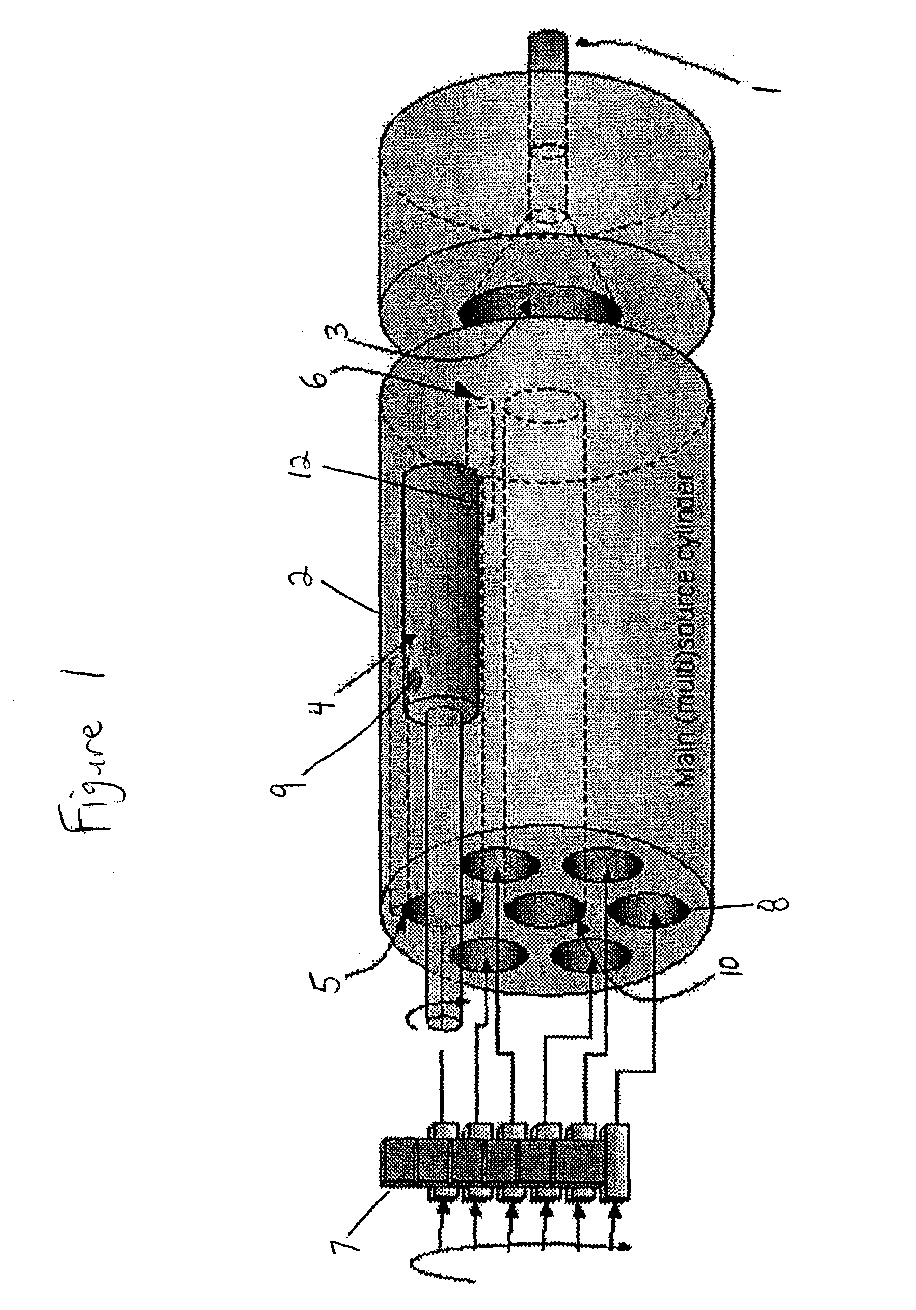
[0050]In Example 1, an embodiment of the device of the invention as seen in FIG. 1 was used to deposit an organic material on a silicon substrate. That is, the device included a single source cell 4 containing an organic material, aluminum tris(8-hydroxyquinoline)(Alq3), and a single nozzle 1 with an inner diameter of about 350 μm. In this example, the distance between the end of the nozzle 1 and the substrate was in the range of about 0.5 to about 1.0 mm, the deposition pressure was about 270 mTorr, and the source cell temperature was about 222° C.

[0051]FIG. 6 shows a photograph of the deposited Alq3 from Example 1 (from an overhead view looking down on the deposited Alq3) showing interference fringes due to the variation in thickness of the deposited Alq3. The width of the deposited Alq3 shown in FIG. 6 is approximately 500 μm.

example 2

[0052]In Example 2, an embodiment of the device of the invention as seen in FIG. 1 was used to deposit an organic material on a silicon substrate. That is, the device included a single source cell 4 containing an organic material, Alq3, and a single nozzle 1. However, in the embodiment of the device used in Example 2, the nozzle 1 had an inner diameter of approximately 50 μm. In this example, the distance between the end of the nozzle 1 and the substrate was in the range of about 0.5 to about 1.0 mm, the deposition pressure was about 270 mTorr, and the source cell temperature was varied within the range of 209° to 225° C.

[0053]FIG. 7 shows a photograph of the deposited Alq3 from Example 2 (from an overhead view looking down on the deposited Alq3) showing interference fringes due to the variation in thickness of the deposited Alq3. The width of the deposited Alq3 shown in FIG. 7 is approximately 100 μm.

[0054]The physical shape of the deposited Alq3 from Example 2 is shown in FIG. 8. ...

example 3

[0055]In Example 3, an embodiment of the device of the invention as seen in FIG. 1 was used to deposit an organic material as part of the fabrication of an OLED. The structure of the fabricated OLED 98 can be seen in FIG. 9.

[0056]The process used to fabricate the OLED 98 shown in FIG. 9 proceeded as follows. A substrate 91 was comprised of a 12.5 mm×12.5 mm×1 mm glass slide. The substrate 91 was pre-coated with a layer 92 of indium tin oxide (ITO), which served as the anode of the OLED 98 structure. A hole injection layer 93 was deposited onto the ITO-layer 92, wherein the hole injection layer 93 comprised about 100 Å of copper phthalocyanine (CuPc). A hole transporting layer 94 was deposited onto the hole injection layer 93, wherein the hole transporting layer 94 comprised about 450 Å of 4,4′-bis[N-(1-napthyl)-N-phenyl-amino] biphenyl (α-NPD).

[0057]Next, an embodiment of the device of the invention as seen in FIG. 1 was used to deposit dots 95 of the organic material Alq3, a green ...


PUM

PropertyMeasurementUnit
Temperatureaaaaaaaaaa
Metallic bondaaaaaaaaaa
Emissivityaaaaaaaaaa

Abstract

A device and a method for facilitating the deposition and patterning of organic materials onto substrates utilizing the vapor transport mechanisms of organic vapor phase deposition is provided. The device includes one or more nozzles, and an apparatus integrally connected to the one or more nozzles, wherein the apparatus includes one or more source cells, a carrier gas inlet, a carrier gas outlet, and a first valve capable of controlling the flow of a carrier gas through the one or more source cells. The method includes moving a substrate relative to an apparatus, and controlling the composition of the organic material and/or the rate of the organic material ejected by the one or more nozzles while moving the substrate relative to the apparatus, such that a patterned organic layer is deposited over the substrate.

Description

CROSS-REFERENCE TO RELATED APPLICATIONS[0001]This patent application is a continuation-in-part of U.S. application Ser. No. 10 / 233,470, filed Sep. 4, 2002, which claims the benefit under 35 U.S.C. § 119(e) of U.S. Provisional Applications No. 60 / 317,215 (filed on Sep. 4, 2001), 60 / 316,264 (filed on Sep. 4, 2001), 60 / 316,968 (filed on Sep. 5, 2001), and 60 / 332,090 (filed on Nov. 21, 2001), and which is related to U.S. application Ser. No. 10 / 233,482 (filed on Sep. 4, 2002). All of these above-mentioned Applications are herein incorporated by reference in their entireties.[0002]The claimed invention was made by, on behalf of, and / or in connection with one or more of the following parties to a joint university-corporation research agreement: Princeton University, The University of Southern California, and Universal Display Corporation. The agreement was in effect on and before the date the claimed invention was made, and the claimed invention was made as a result of activities undertak...

Claims


Application Information

Patent Timeline
IPC IPC(8): C23C16/00C23C14/04C23C14/12C23C14/24H01L51/00H01L51/40H01L51/56
CPCC23C14/04C23C14/042C23C14/12C23C14/228H01L51/001H01L51/0013C23C14/24H01L51/56H01L51/0008H01L51/0021H10K71/16H10K71/164H10K71/18H10K71/60H10K71/40H10K71/00
Inventor SHTEIN, MAXFORREST, STEPHEN R.BENZINGER, JAY B.
Owner THE TRUSTEES FOR PRINCETON UNIV
Why Eureka
Try Eureka