Semiconductor device and display device

a display device and semiconductor technology, applied in non-linear optics, instruments, optics, etc., can solve the problems of large area, complicated wiring between tfts, and ineffective multi-layer technology, so as to reduce the arrangement area required, the ground voltage rises drastically, and the arrangement area is reduced.

Active Publication Date: 2008-08-05
SEMICON ENERGY LAB CO LTD
View PDF5 Cites 14 Cited by
  • Summary
  • Abstract
  • Description
  • Claims
  • Application Information

AI Technical Summary

Benefits of technology

[0012]The present invention is made in view of above-described problems in order to provide a semiconductor device and a display device which include lightweight, thin, and high performance functional circuits by the manufacturing functional circuits formed by using TFTs with as few masks as possible while occupying as small area as possible for wirings of the functional circuits, and further keeping the power supply voltage and the ground voltage equal at each part of the functional circuits.
[0013]In a functional circuit which is formed by using TFTs in a semiconductor device and a display device of the present invention, a power supply wiring and a ground wiring are formed in a comb-like arrangement by using the second wiring and the tips of the wirings formed in the comb-like arrangement are electrically connected with the first wiring and a contact between the first wiring and the second wiring. By using the first wiring, the contact between the first wiring and second wiring, and the second wiring, the power supply wiring and the ground wiring are formed in a grid-like arrangement. The extends of a drop in a power supply voltage and a rise in ground voltage can be drastically decreased in the grid-like arrangement by comparison with the case where the grid-like arrangement is not employed. Furthermore, in the case where the width of wiring are thinned, a drop in a power supply voltage and a rise in a ground voltage can be suppressed to the extent in the case where a grid-like arrangement is not employed, resulting in a drastic decrease in the arrangement area required for the power supply wiring and the ground wiring. Moreover, an electrostatic capacitor can be formed between the power supply wiring and the ground wiring at the same time of forming the power supply wiring and the ground wiring. The electrostatic capacitor suppresses the change in the absolute value of potential due to a momentary change in potential, therefore the electrostatic capacitor is preferably provided in terms of a circuit operation.
[0014]Thus, a semiconductor device and a display device are provided which include functional circuits by manufacturing the functional circuits formed by using TFTs with as few masks as possible while occupying as a small area as possible for wirings of the functional circuits, and further keeping the power supply voltage and the ground voltage equal at each part of the functional circuits. In this manner, a semiconductor device and a display device which are higher in performance and added value can be provided at a low cost.

Problems solved by technology

Therefore, the conventional multilayer technology is not necessarily an efficient method when the functional circuit formed by using TFTs is manufactured.
To realize an advanced functional circuit, lead wirings between TFTs are very complicated, which lead to occupying a large area.
As a result, a power supply voltage drops rapidly in a local circuit of high current consumption.
A net power supply voltage applied to the TFT is decreased drastically in the area that the power supply voltage is dropped, and therefore it cannot provide as much TFT performance as expected.
This may lead to a malfunction of circuit or a problem such that the designed operation frequency might not be obtained.
Similarly, a ground voltage rises, which may lead to a malfunction of circuit or a problem such that the designed operation frequency might be obtained.

Method used


Image

  • Semiconductor device and display device
  • Semiconductor device and display device
  • Semiconductor device and display device

Examples


embodiment mode 1

[Embodiment Mode 1]

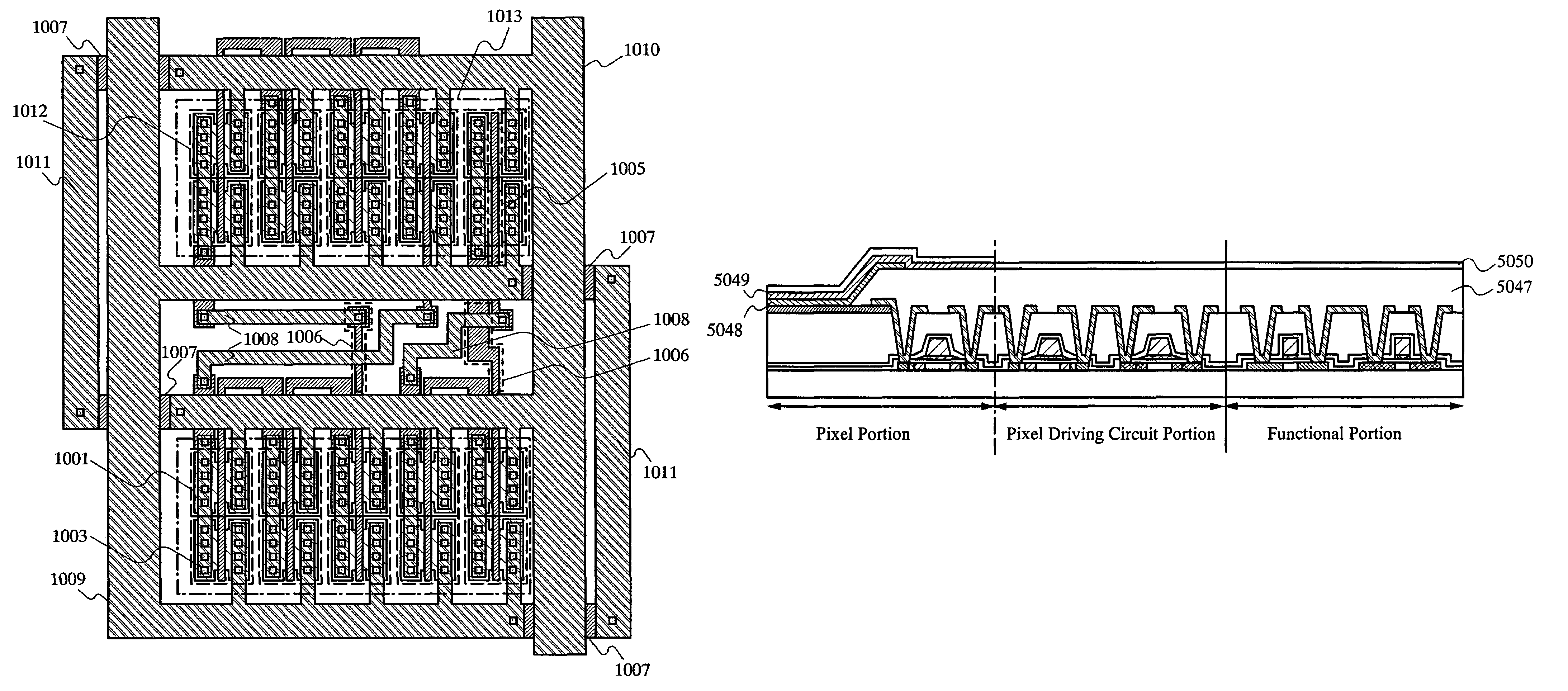
[0064]In this embodiment mode, a mask layout of a functional circuit in a semiconductor device and a display device according to the present invention is described. FIG. 1 shows a mask layout of this embodiment mode.

[0065]FIG. 1 shows an active layer 1001 which corresponds to a channel region, a source region, and a drain region of a TFT, a first wiring layer including a gate wiring 1005, a wiring 1006 between TFTs, and a first wiring 1007 which forms a power supply wiring or a ground wiring in a grid-like arrangement (hereinafter referred to as a first wiring for forming in a grid-like arrangement), a contact 1003 for connecting the first wiring and a second wiring or the active layer and the second wiring electrically, a second wiring layer including of a wiring 1008 between TFTs, a power supply wiring 1009, a ground wiring 1010, and the second wiring 1011 which forms a power supply wiring or a ground wiring in a grid-like arrangement (hereinafter referred to as...

embodiment mode 2

[Embodiment Mode 2]

[0073]In this embodiment mode, a mask layout of a functional circuit in a semiconductor device and a display device according to the present invention which is different from Embodiment Mode 1 is described. FIG. 3 shows a mask layout of this embodiment mode. It is to be noted that portions which are identical in FIG. 1 are denoted by the same reference symbols.

[0074]FIG. 3 shows the active layer 1001 which corresponds to a channel region, a source region, and a drain region of a TFT, the first wiring layer including the gate wiring 1005, the wiring 1006 between TFTs, and the first wiring 1007 which forms a power supply wiring or a ground wiring in a grid-like arrangement (hereinafter referred to as a first wiring for forming in a grid-like arrangement), the contact 1003 for connecting the first wiring and a second wiring or the active layer and the second wiring electrically, the second wiring layer including the wiring 1008 between TFTs, the power supply wiring 1...

embodiment

[Embodiment]

[Embodiment 1]

[0080]In this embodiment as an example of a display device of the invention, a display device in which a CPU, an SRAM and the like are formed over the same substrate is explained.

[0081]FIG. 4 shows a top view of a display device of the embodiment. The display device in FIG. 4 includes a display portion 551 and a functional circuit portion 552 which are formed by using TFTs formed over a substrate 500 having an insulating surface. The display portion 551 includes a pixel portion 501, a scanning line driver circuit 502, and a signal line driver circuit 503. Also, the functional circuit portion 552 includes a CPU 507 and an SRAM (memory circuit) 504. In the display portion 551, the pixel portion 501 displays an image. Further, the scanning line driver circuit 502 and the signal line driver circuit 503 control an input of a video signal to each pixel in the pixel portion 501. The SRAM 504 is formed by using a plurality of memory cells (not shown) arranged in ma...


PUM

PropertyMeasurementUnit
thicknessaaaaaaaaaa
thicknessaaaaaaaaaa
thicknessaaaaaaaaaa

Abstract

It is an object of the invention to provide a thin, lightweight, high performance, and low in cost semiconductor device and a display device by reducing an arrangement area required for a power supply wiring and a ground wiring of a functional circuit and decreasing a drop in power supply voltage and a rise in ground voltage.
In the functional circuit of the semiconductor device and the display device, a power supply wiring and a ground wiring are formed in a comb-like arrangement, and the tips thereof are electrically connected with a first wiring, a second wiring, and a contact between the first wiring and the second wiring, thereby forming in a grid-like arrangement. The drop in power supply voltage and the rise in ground voltage can be decreased and the arrangement area can be decreased in the grid-like arrangement.

Description

BACKGROUND OF THE INVENTION[0001]1. Field of the Invention[0002]The present invention relates to a semiconductor device and a display device. Specifically, the present invention relates to a semiconductor device and a display device which are lightweight, thin, and can realize a high performance at a low cost.[0003]2. Description of the Related Art[0004]Recently, research and development have eagerly been made on a display device for which a thin film transistor (TFT) is fabricated by using a polycrystalline silicon thin film as an active layer and provides as a switching element in a pixel portion, and an active matrix display device for which a circuit is provided so as to drive a pixel in the periphery of a pixel portion.[0005]Furthermore, by using such high performance TFTs, research and development for providing a functional circuit represented by a large scale integrated circuit (LSI) over an insulating substrate have been started. The functional circuit conventionally could o...

Claims


Application Information

Patent Timeline
Patent Type & Authority Patents(United States)
IPC IPC(8): H01L27/01H01L29/276G02F1/1362H01L21/77H01L21/84H01L27/10H01L27/12
CPCG02F1/13454H01L27/124
Inventor KUROKAWA, YOSHIYUKI
Owner SEMICON ENERGY LAB CO LTD
Why Eureka
Try Eureka