Method of manufacturing silicon rich oxide (SRO) and semiconductor device employing SRO

a manufacturing method and technology of silicon rich oxide, applied in semiconductor devices, chemical vapor deposition coatings, coatings, etc., can solve the problems of poor control of the si:o ratio within the sro layer, poor step coverage, ald process, etc., to improve the control of the silicon:oxygen ratio and the effect of improving the step coverag

Active Publication Date: 2008-08-12
SAMSUNG ELECTRONICS CO LTD
View PDF2 Cites 56 Cited by
  • Summary
  • Abstract
  • Description
  • Claims
  • Application Information

AI Technical Summary

Benefits of technology

[0007]Example embodiments of the invention include methods of manufacturing silicon rich oxide (SRO) layers that provide both improved step coverage and improved control over the silicon:oxygen ratio within the resulting SRO materials. Other example embodiments of the invention include methods of manufacturing semiconductor devices that incorporate such improved SRO materials.

Problems solved by technology

CVD processes, however, while generally providing better control over the Si:O ratio than ALD processes, tend to exhibit poor step coverage due to plasma shielding effect.
Conversely, ALD processes, while generally providing better step coverage than CVD processes, tend to exhibit poor control over the Si:O ratio within the SRO layer due to the nature of the exchange reaction between a precursor, for example, tetraethoxysilane (TEOS, (Si(OC2H5)4, also referred to in the alternative as tetraethosiloxane or tetraethylorthosilicate), and an oxidation agent, for example, H2O.

Method used


Image

  • Method of manufacturing silicon rich oxide (SRO) and semiconductor device employing SRO
  • Method of manufacturing silicon rich oxide (SRO) and semiconductor device employing SRO
  • Method of manufacturing silicon rich oxide (SRO) and semiconductor device employing SRO

Examples


Embodiment Construction

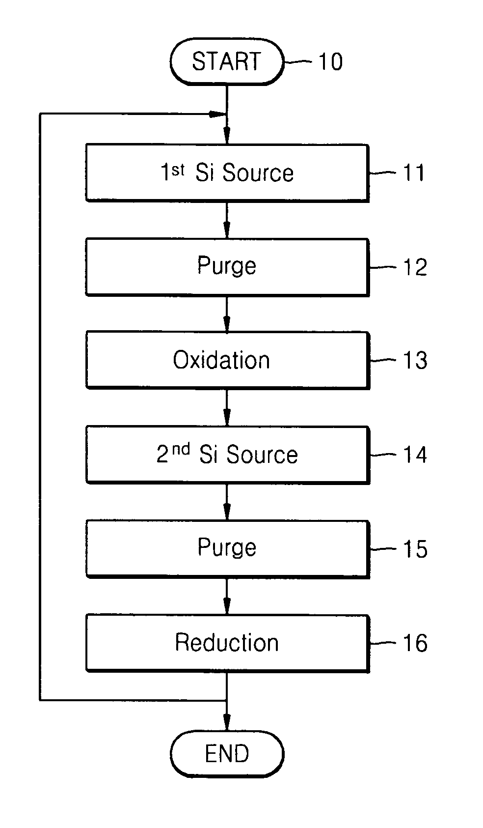
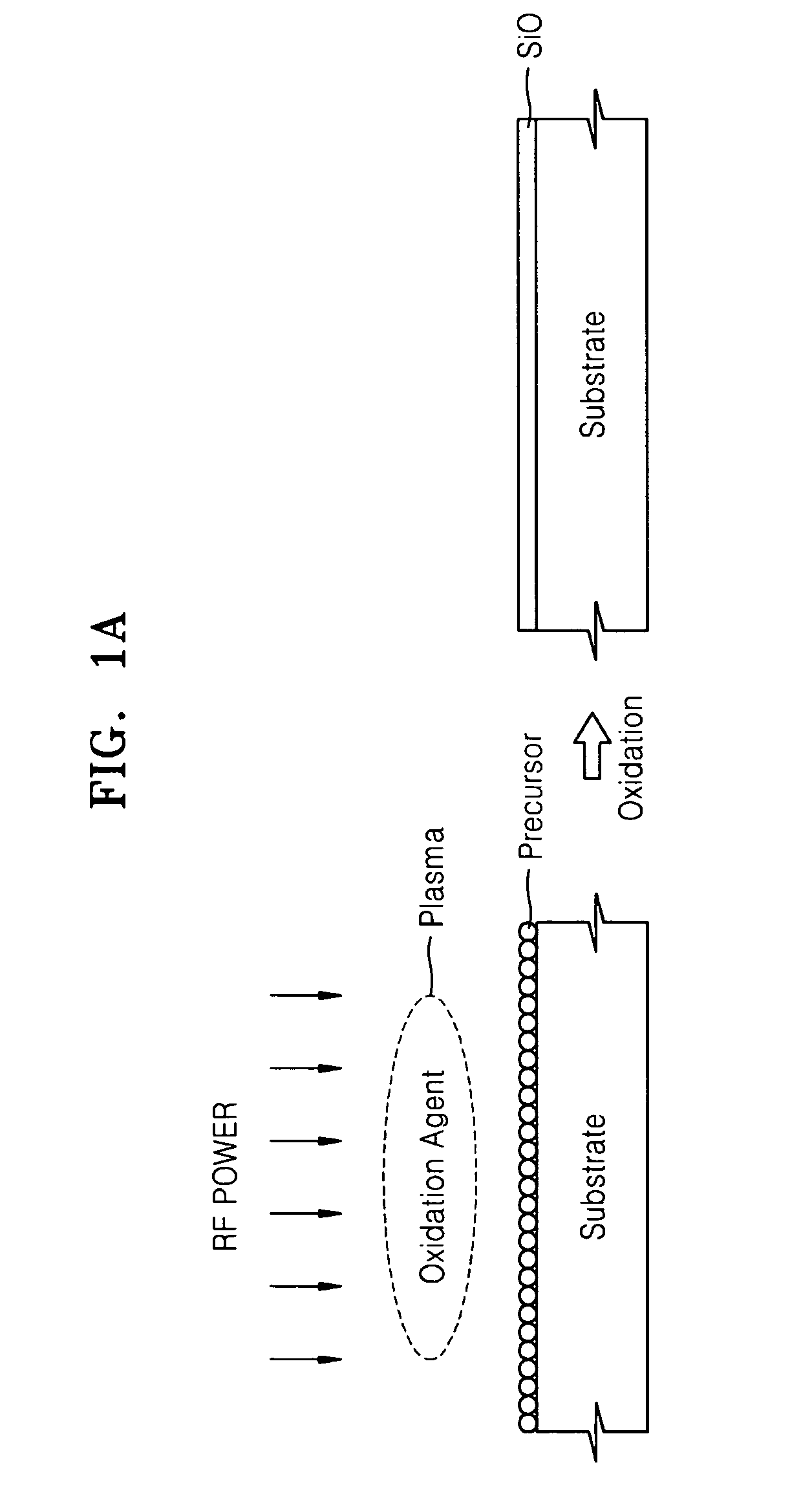
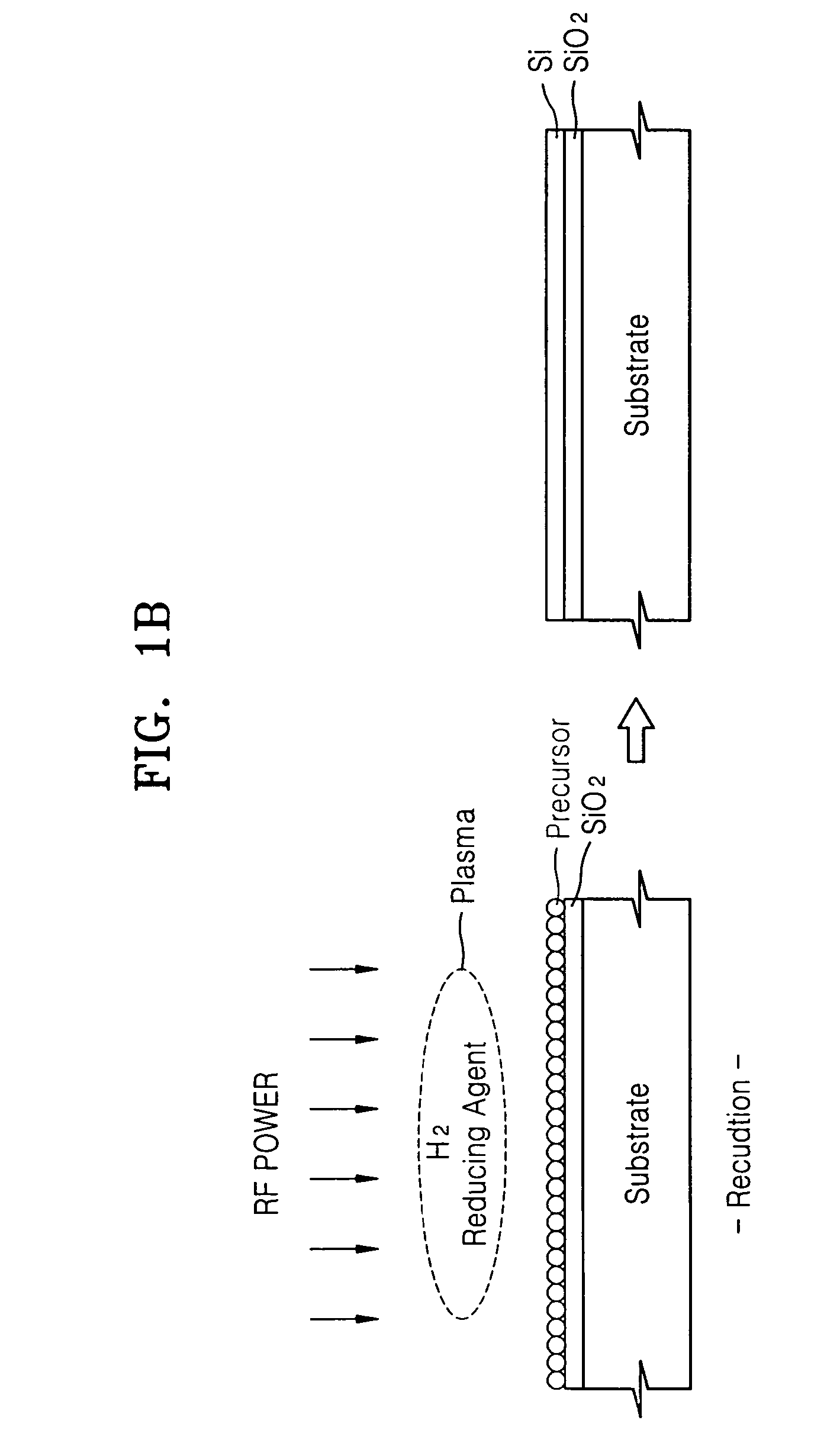
[0024]A method of manufacturing silicon rich oxide (SRO) according to an example embodiment of the invention includes forming both a silicon oxide layer, for example, SiO2, and a silicon layer using atomic layer deposition (ALD) processes as shown in FIGS. 1A and 1B. More specifically, after a silicon precursor is absorbed onto a substrate, an appropriate reaction gas is introduced into the reaction chamber in which RF power is applied to the reaction gas to generate a plasma. When the reaction gas is H2O, an oxidizing plasma is generated. When the reaction gas is H2, hydrogen plasma is generated. When reaction energy is supplied to the precursor by the oxidizing plasma and the reducing plasma, the corresponding oxidation and reduction reactions are initiated between the absorbed silicon precursor molecule and the reaction gases to produce a silicon oxide layer, for example, SiO2, or a silicon layer respectively. The ALD formation sequences for the silicon oxide layer(s) and the sil...


PUM

PropertyMeasurementUnit
pressureaaaaaaaaaa
temperatureaaaaaaaaaa
stress voltageaaaaaaaaaa

Abstract

Provided are methods for manufacturing silicon rich oxide (SRO) layers useful in the fabrication of semiconductor devices, for example, non-volatile memory devices, and methods for fabricating semiconductor devices incorporating such SRO layers. The methods include absorbing a first silicon source gas onto the substrate, oxidizing the first absorbed layer to form a silicon oxide layer, absorbing a second silicon source gas onto the substrate and reducing the second absorbed layer to form a silicon layer. The combination of the silicon oxide layer(s) and the silicon layer(s) comprise, in turn, a composite SRO layer. These manufacturing methods facilitate control of the oxygen concentration in the SRO, the relative thicknesses of the silicon oxide and silicon layers, and provides improved step coverage, thus allowing the manufacturing of high quality semiconductor devices.

Description

PRIORITY STATEMENT[0001]This application claims priority under 35 U.S.C. § 119 from Korean Patent Application No. 10-2005-0088713, filed on Sep. 23, 2005, in the Korean Intellectual Property Office, the disclosure of which is incorporated herein in its entirety by reference.BACKGROUND OF THE INVENTION[0002]1. Field of the Invention[0003]The invention relates to methods for manufacturing silicon rich oxide (SRO), and more particularly, to methods for manufacturing semiconductor devices incorporating one or more regions of SRO.[0004]2. Description of the Related Art[0005]Charge storage devices incorporating SRO have been receiving increasing attention as a result of various advantages provided by the SRO when utilized as a charge trapping layer. Controlling the ratio of Si and SiO2 in the SRO material incorporated in dynamic random access memory (DRAM) devices can provide improved electrical characteristics relative to conventional DRAM devices. In particular, annealing a SRO having a...

Claims


Application Information

Patent Timeline
Patent Type & Authority Patents(United States)
IPC IPC(8): H01L21/31
CPCC23C16/401C23C16/45525C23C16/45529H01L21/32055H01L21/3141H01L29/66833H01L29/66825H01L21/02164H01L21/02274H01L21/022H01L21/0228
Inventor LEE, JUNG-HYUNBANG, SANG-BONG
Owner SAMSUNG ELECTRONICS CO LTD
Why Eureka
Try Eureka