Semiconductor memory arrangement with branched control and address bus

a memory controller and branched control technology, applied in the field of semiconductor memory, can solve the problems of too narrow bandwidth for high data rates of 1.6 gbit/s/pin, too low structural density, etc., and achieve the effect of reducing the latency time of re-driving control and address data of memory controllers

Inactive Publication Date: 2008-08-12
POLARIS INNOVATIONS
View PDF5 Cites 26 Cited by
  • Summary
  • Abstract
  • Description
  • Claims
  • Application Information

AI Technical Summary

Benefits of technology

[0018]When a semiconductor memory arrangement is arranged on a semiconductor memory module, the semiconductor memory arrangement is fit with semiconductor memory chips arranged on a front side and a back side, whereby a signal line bus for control and address signals is connected to the semiconductor memory chips on t

Problems solved by technology

A major disadvantage of the flyby topology is the too narrow bandwidth for hig

Method used


Image

  • Semiconductor memory arrangement with branched control and address bus
  • Semiconductor memory arrangement with branched control and address bus
  • Semiconductor memory arrangement with branched control and address bus

Examples


Embodiment Construction

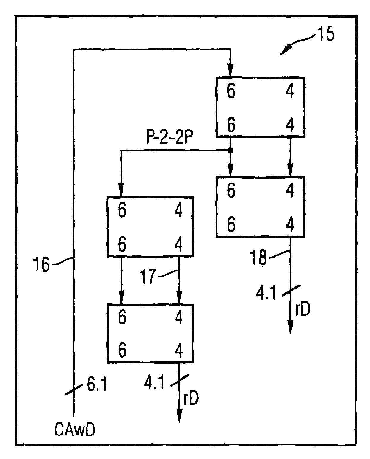
[0026]Referring to FIG. 1, the signal line bus topology in an embodiment of the semiconductor memory arrangement according to the invention is shown schematically. Accordingly, on a x4-based DIMM semiconductor memory module, identified by reference number 1, 8 DRAM memory chips 2 are provided on a front side and 8 DRAM memory chips on a back side of the semiconductor memory module. DRAMs 1.1, 1.2, 1.3, 1.4 allocated to a first rank and DRAMs 2.1, 2.2, 2.3, 2.4 allocated to a second rank are arranged on the front side of the DIMM module 1. DRAMs 3.1, 3.2, 3.3, 3.4 allocated to a third rank and DRAMs 4.1, 4.2, 4.3, 4.4 allocated to a fourth rank are arranged on the back side of the DIMM module 1.

[0027]The DIMM module 1 is connected to a memory controller 2 by a first uni-directional signal line bus 3 for control and address signals, a second uni-directional signal line bus 4 for control and address signals, and four unidirectional combined signal line busses 5 for write and read data ...


PUM


Abstract

A semiconductor memory arrangement for operation in a data memory system with at least one semiconductor memory chip for the storage of user data includes a memory controller for control of the at least one semiconductor memory chip, and at least one unidirectional signal line bus for control and address signals connected with the memory controller and branching at least once. The at least once branching bus directly connecting at least one semiconductor memory chip with the memory controller and connecting the semiconductor memory chips among each other.

Description

FIELD OF THE INVENTION[0001]The present invention relates to semiconductor memories and, more particularly, to a semiconductor memory arrangement for a data memory system with a plurality of semiconductor memory chips for user data connected to a memory controller by a control and address bus.BACKGROUND[0002]Considering the continuously increasing processor working speed in computers, such as personal computers, workstations, and servers, it is indispensable to increase the working speed of semiconductor memories in order to prevent losses of performance. Consequently, memory modules with very fast and high density memory components, DDR-DRAMs (Double Data Rate Dynamic Random Access Memory) of generations 1, 2, and 3 have been developed in recent years, in which the working speed and structure density were continually improved.[0003]In a conventional DIMM semiconductor memory module with DDR-DRAMs serving as semiconductor memory chips, for example, two or four ranks per semiconducto...

Claims


Application Information

Patent Timeline
IPC IPC(8): G11C7/00
CPCG11C5/063
Inventor RUCKERBAUER, HERMANNWEISS, CHRISTIANSCHLEDZ, RALFSTECKER, JOHANNES
Owner POLARIS INNOVATIONS
Why Eureka
Try Eureka