Semiconductor device having a multilayer interconnection structure and fabrication method thereof

a technology of interconnection structure and semiconductor device, which is applied in the direction of semiconductor device, semiconductor/solid-state device details, electrical apparatus, etc., can solve problems such as signal delay, and achieve the effect of increasing the length of diffusion of metal elements

Inactive Publication Date: 2008-08-26
FUJITSU SEMICON LTD
View PDF19 Cites 29 Cited by
  • Summary
  • Abstract
  • Description
  • Claims
  • Application Information

AI Technical Summary

Benefits of technology

[0044]According to the present invention, diffusion of the metal element toward the surface of the metal interconnection pattern along such a crystal grain boundary is suppressed by introducing oxygen into the crystal grain boundaries in the metal interconnection pattern formed so as to fill the interconnection groove in the interlayer insulation film. Thereby, formation of defects such as void caused in the metal interconnection patterns constituting such a multilayer interconnection structure during the operation of the semiconductor device having such a multilayer interconnection structure such as conduction test, is suppressed. Further, according to the present invention, projections and depressions are formed on the surface of the metal interconnection pattern in correspondence to the morphology of the crystal grains in the metal interconnection pattern as a result of formation and removal of the oxide film, while formation of such projections and depressions increases the length of diffusion of the metal element along the surface of the metal interconnection pattern. Thereby, escaping of the metal atoms to the outside of the metal interconnection pattern by diffusion is suppressed.

Problems solved by technology

On the other hand, with such increase of integration density, there arises the problem of signal delay in such a semiconductor integrated circuit caused by wiring resistance and wiring capacitance.

Method used


Image

  • Semiconductor device having a multilayer interconnection structure and fabrication method thereof
  • Semiconductor device having a multilayer interconnection structure and fabrication method thereof
  • Semiconductor device having a multilayer interconnection structure and fabrication method thereof

Examples


first embodiment

[0061]Hereinafter, a first embodiment of the present invention will be explained.

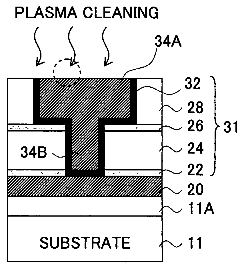
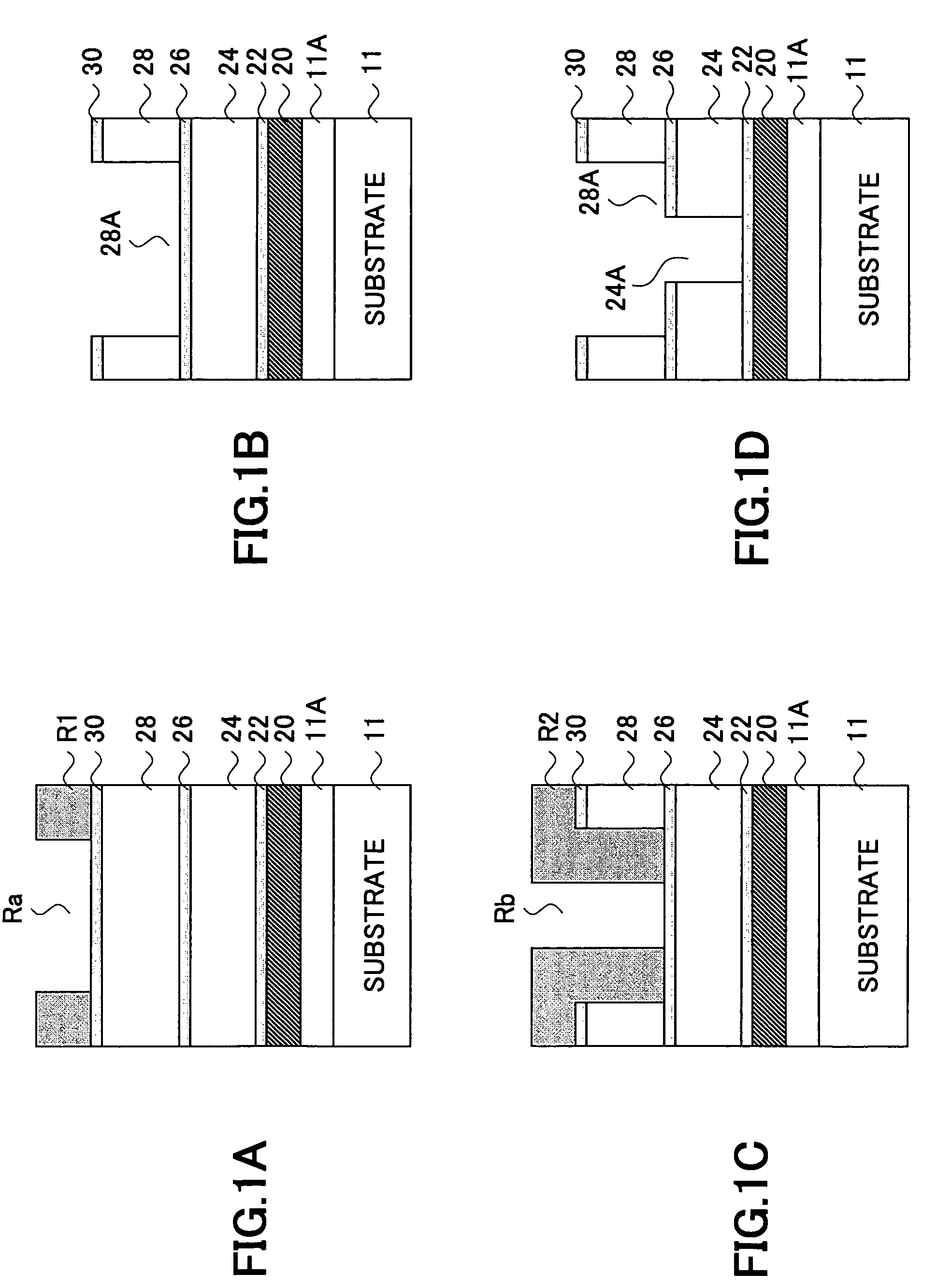
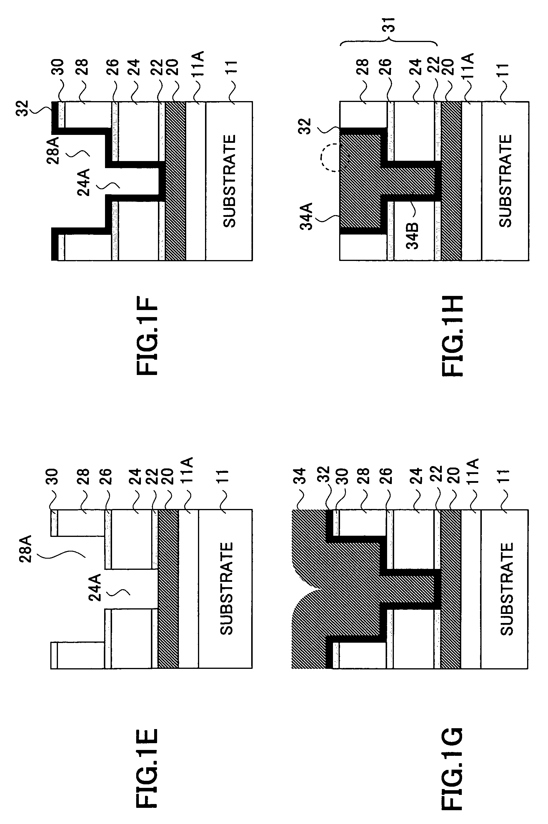
[0062]In the present embodiment, the process steps of FIGS. 1A-1H explained previously are conducted, and there is obtained a structure shown in FIG. 1H in which the Cu pattern 34A is formed in the interlayer insulation film 28 via the barrier metal film 32 and the Cu plug 34B is formed in the interlayer insulation film 24 via the barrier film 32.

[0063]Here, it should be noted that the present invention uses a low-K dielectric aromatic hydrocarbon polymer marketed from Dow Chemical Inc. with the trademark SiLK for the interlayer insulation films 24 and 28 and an SiC film formed by a plasma CVD. process for the etching stopper film 22. Thereby, it is preferable to carry out the plasma CVD process for forming the SiC film at the substrate temperature of about 400° C. by using trimethyl silane for the source material while supplying a high frequency power of 50-700 W. For the barrier metal film 32, it is p...

second embodiment

[0079]Next, the process of forming a multilayer interconnection structure according to a second embodiment of the present invention will be explained.

[0080]In the present embodiment, the process steps of FIGS. 1A-1G explained previously are conducted at first, and thus, the Cu layer 34 is formed on the barrier metal film 32 by an electrolytic plating process as shown in FIG. 1G, such that the Cu layer 34 fills the interconnection trench 28A and the via-hole 24A.

[0081]As explained previously, the low-K dielectric aromatic hydrocarbon polymer such as the one marketed from the Dow Chemical Inc. under the trademark SiLK is used for the low dielectric insulation films 24 and 28, while an SiC film formed by a plasma CVD process is used for the etching stopper film 22. Further, an ordinary barrier metal film in which a TaN film and a Ta film are laminated is formed for the barrier metal film 32.

[0082]In the present embodiment, too, it is possible to use films other than the organic hydroca...


PUM


Abstract

A multilayer interconnection structure includes a first interlayer insulation film, a second interlayer insulation film formed over the first interlayer insulation film, an interconnection trench formed in the first interlayer insulation film and having a sidewall surface and a bottom surface covered with a first barrier metal film, a via-hole formed in the second interlayer insulation film and having a sidewall surface and a bottom surface covered with a second barrier metal film, an interconnection pattern filling the interconnection trench, and a via-plug filling the via-hole, wherein the via-plug makes a contact with a surface of the interconnection pattern, the interconnection pattern has projections and depressions on the surface, the interconnection pattern containing therein oxygen atoms along a crystal grain boundary extending from the surface toward an interior of the interconnection pattern with a concentration higher than a concentration at the surface.

Description

CROSS-REFERENCE TO RELATED APPLICATIONS[0001]The present invention is a continuation application filed under 35 U.S.C. 111(a) claiming benefit under 35 U.S.C. 120 and 365(c) of PCT application JP2002 / 13677 filed on Dec. 26, 2002, the entire contents of which are incorporated herein as reference.BACKGROUND OF THE INVENTION[0002]The present invention relates to semiconductor devices and fabrication method thereof and more particularly to a semiconductor device having a multilayer interconnection structure and fabrication method thereof.[0003]With progress in the art of device miniaturization, integration density of semiconductor integrated circuits is increasing year by year. On the other hand, with such increase of integration density, there arises the problem of signal delay in such a semiconductor integrated circuit caused by wiring resistance and wiring capacitance. In view of this problem of signal delay, investigations are being made these days about the technology of using low-...

Claims


Application Information

Patent Timeline
Patent Type & Authority Patents(United States)
IPC IPC(8): H01L21/4763H01L21/311H01L21/461H01L21/3205H01L21/768H01L23/52H01L23/522H01L23/532
CPCH01L21/76807H01L21/76838H01L21/7684H01L21/76888H01L21/76892H01L23/5226H01L23/53228H01L23/53238H01L23/53295H01L2924/0002H01L2924/3011H01L2924/00
Inventor YAMAMOTO, TAMOTSUWATANI, HIROFUMIKITADA, HIDEKIHORIUCHI, HIROSHIMIYAJIMA, MOTOSHU
Owner FUJITSU SEMICON LTD
Why Eureka
Try Eureka