Multi-wavelength GaN-based core-shell nanorod LED device structure and preparation method thereof

A technology of LED devices and nanorods, applied in semiconductor devices, electrical components, circuits, etc., can solve problems such as device performance degradation and damage, and achieve the effects of low cost, improved recombination probability, and reduced polarization electric field.

Inactive Publication Date: 2019-11-12
张士英
View PDF4 Cites 6 Cited by
  • Summary
  • Abstract
  • Description
  • Claims
  • Application Information

AI Technical Summary

Problems solved by technology

Compared with wet etching, dry etching has the advantages of good anisotropy and line width control, but due to the high energy of plasma, it will bring great damag

Method used


Image

  • Multi-wavelength GaN-based core-shell nanorod LED device structure and preparation method thereof
  • Multi-wavelength GaN-based core-shell nanorod LED device structure and preparation method thereof

Examples


Embodiment Construction

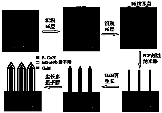
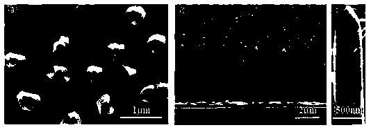
[0044] The present invention will be further elaborated below in conjunction with the accompanying drawings and specific embodiments. Such as figure 1 Fabrication flow chart of the multi-wavelength GaN-based core-shell nanorod LED device structure shown, figure 2 (a) SEM photo of Ni nano-islands; (b) SEM photo of the cross-section of GaN-based core-shell nanorod LED device structure; (c) cross-section of a single GaN-based core-shell nanorod LED device structure Scanning electron microscope photo. A method for preparing a multi-wavelength GaN-based core-shell nanorod LED device structure of the present invention comprises the following steps:

[0045] 1) The original sample is a GaN film with a thickness of about 20 μm grown by HVPE on a (0001) sapphire substrate. The sample is ultrasonically cleaned and dried in acetone, alcohol, and deionized water; Its surface is coated with a 25nm thick Ni metal film;

[0046] 2) Then put the Ni / GaN / sapphire sample into a high-temper...


PUM

PropertyMeasurementUnit
Thicknessaaaaaaaaaa
Sizeaaaaaaaaaa
Heightaaaaaaaaaa

Abstract

The invention discloses a multi-wavelength GaN-based core-shell nanorod LED device structure and a preparation method thereof. A self-organized Ni nano island formed by high-temperature ammonia annealing is used as a template to prepare GaN nanorods with high consistency; a wet etching technology is then used to repair dry etching damage on the nanorod surface, n-type GaN regrowth is carried out on the obtained GaN nanorod array, and a six-sided pillar with a top cone is formed; multi-quantum well layers and P-type GaN layers coating the surfaces of the GaN nanorod array are sequentially stacked to obtain the multi-wavelength GaN-based core-shell nanorod LED device structure. The GaN nanorod array and the multi-quantum well layers and the P-type GaN layers coating the surfaces of the GaN nanorod array form the three-dimensional core-shell structure, which can generate more photons at the same current density and improve the internal quantum efficiency of an LED epitaxial structure. Themethod does not require a patterned substrate, the process cost is low, the preparation is simple and easy to implement, large-scale production is facilitated, and the core-shell nanorod array can bewidely applied to optoelectronic devices and microelectronic devices.

Description

technical field [0001] The invention relates to the field of semiconductor light-emitting devices, in particular to a multi-wavelength GaN-based core-shell nanorod LED device structure and a preparation method thereof. Background technique [0002] Among wide-bandgap semiconductors with direct bandgap, GaN-based semiconductors have the most development potential and development prospects. With their wide bandgap [0.64 eV (InN), 3.4eV (GaN), 6.2eV, (AlN)] and superior The performance (thermal stability, chemical stability and high thermal conductivity, etc.) has become a hot spot and focus in the research of optoelectronic materials and devices in recent years. GaN-based white light LEDs have the advantages of long service life, small size, high photoelectric conversion efficiency and low heat generation, and have been widely used in instrument and equipment lighting, aircraft lighting, automotive lighting, mobile phones, and decorative lighting. [0003] Traditional white L...

Claims


Application Information

Patent Timeline
IPC IPC(8): H01L33/06H01L33/32H01L33/18H01L33/00
CPCH01L33/007H01L33/06H01L33/18H01L33/32
Inventor 张士英徐庆君
Owner 张士英
Why Eureka
Try Eureka