Semiconductor device

a technology of semiconductor devices and semiconductors, applied in pulse manipulation, pulse techniques, instruments, etc., can solve the problems of increasing data access time, and increasing the load of the global data bus line, so as to increase the data transfer rate in transferring data output, reduce the swing width of data, and enhance the effect of high-frequency operation characteristics

Active Publication Date: 2008-09-09
SK HYNIX INC
View PDF12 Cites 11 Cited by
  • Summary
  • Abstract
  • Description
  • Claims
  • Application Information

AI Technical Summary

Benefits of technology

[0006]A semiconductor device increases the data transfer rate in transferring data output from an input / output sense amplifier via a global data bus line by reducing the swing width of the data placed on the global data bus line, thereby achieving an enhancement in high-frequency operation characteristics while suppressing generation of data errors.

Problems solved by technology

However, where the global data bus line is constituted by equivalent resistors, capacitors, etc, so that the load of the global data bus line is large. there is a problem in that a significant increase in data access time occurs when the data transferred via the global data bus line is fully swung between the external voltage and the ground voltage, as mentioned above, namely. when the swing width of the data is large.
Such an increase in data transition time causes an increase in data access time, and thus, a degradation in high-frequency operation characteristics.
For this reason, the data receiver 120 may incorrectly sense the low level of data, so that data errors may occur.

Method used


Image

  • Semiconductor device
  • Semiconductor device
  • Semiconductor device

Examples


Embodiment Construction

[0050]Hereinafter, the various exemplary embodiments are described. These embodiments are used only for illustrative purposes, and the present invention is not limited thereto.

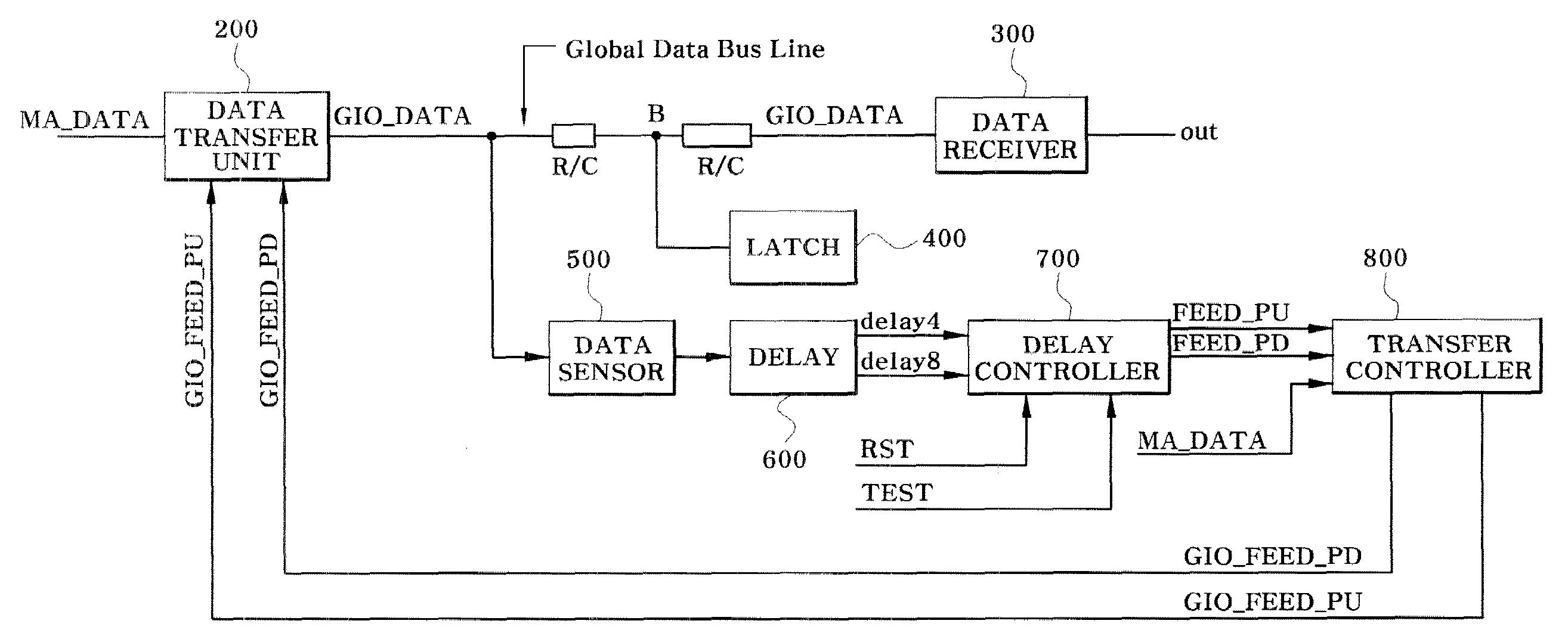
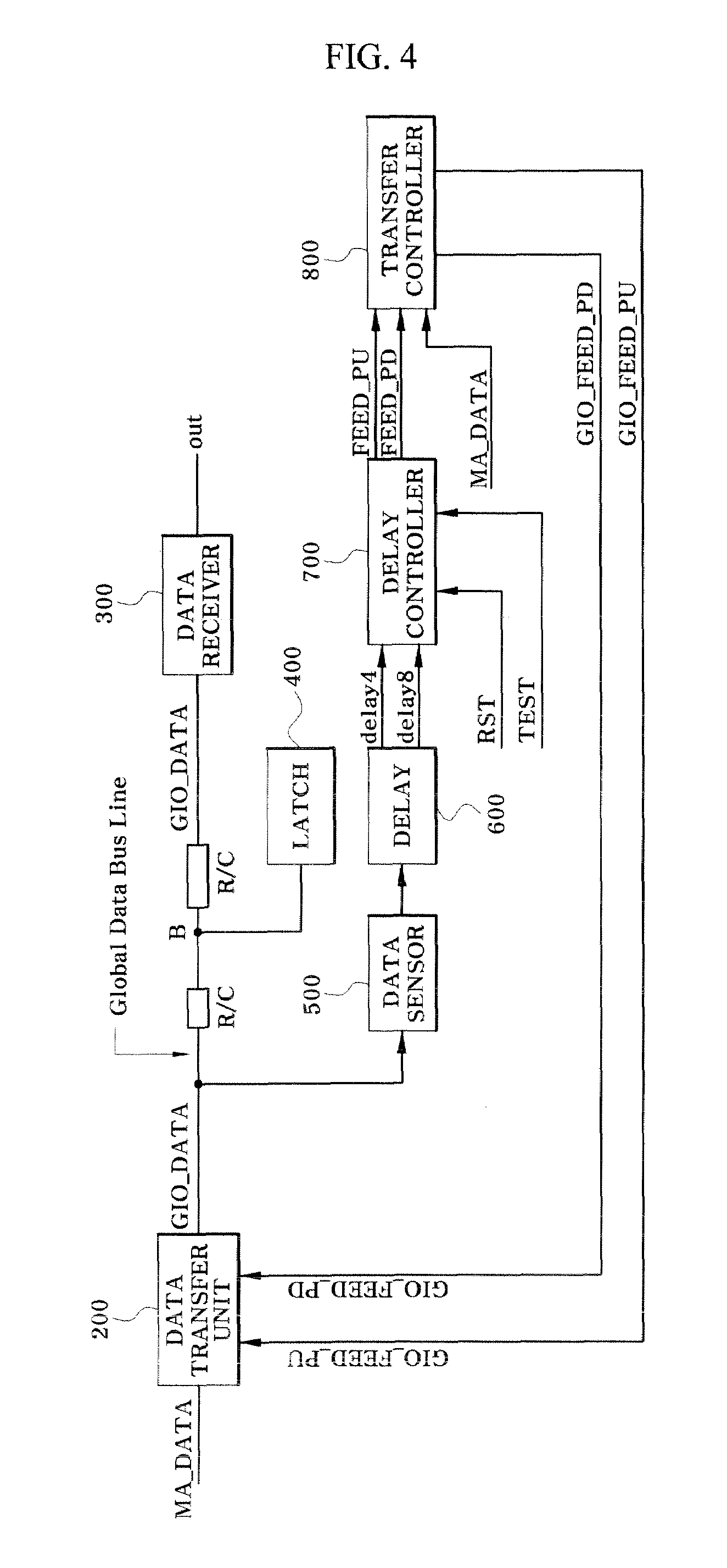
[0051]FIG. 4 illustrates a configuration of a semiconductor device according to an exemplary embodiment. FIGS. 5 to 8 illustrate configurations of constituent elements of the semiconductor device according to the exemplary embodiment.

[0052]As shown in FIG. 5, the semiconductor device according to the exemplary embodiment includes a data transfer unit 200 which receives data MA_DATA output from an input / output (I / O) sense amplifier, and outputs data GIO_DATA, obtained after driving the data MA_DATA to a predetermined level, to a global data bus line, a data receiver 30 which receives the data GIO_DATA transferred via the global data bus line, and a delay 600 which outputs delay signals delay4 and delay8 respectively obtained after delaying the data GIO_DATA output from the data transfer unit 200 for predetermin...


PUM


Abstract

A semiconductor device is disclosed which increases the data transfer rate in transferring data output from an input / output sense amplifier via a global data bus line by reducing the swing width of the data placed on the global data bus line. The semiconductor device may include a data transfer unit which receives first data, and outputs second data obtained by driving the first data to a predetermined level to a data transfer line; a data receiver which receives the second data transferred via the data transfer line; a delay which outputs a plurality of delay signals respectively obtained by delaying the second data outputted from the data transfer unit by different delay periods; a delay controller which selects one of the delay signals in accordance with an operation mode of the semiconductor device, and outputs at least one adjustment signal for adjusting a driving period of the data transfer unit for the first data based on the delay period of the selected delay signal; and a transfer controller which receives the first data and the at least one adjustment signal, and outputs at least one transfer control signal for controlling the operation of the data transfer unit, based on the received first data and adjustment signal.

Description

TECHNICAL FIELD[0001]This patent relates to a semiconductor device, and, more particularly, to a semiconductor device which increases the data transfer rate in transferring data output from an input / output sense amplifier via a global data bus line by reducing the swing width of the data placed on the global data bus line, thereby achieving an enhancement in high-frequency operation characteristics.DESCRIPTION OF THE RELATED ART[0002]Dynamic random access memories (DRAMs) are well known as a volatile memory device which includes cells each having one transistor and one capacitor to store data. Basic functions of such a DRAM, namely, data inputting / outputting operations, are carried out in accordance with ON / OFF of word lines connected to the gates of transistors in the cells of the DRAM.[0003]In a general DRAM memory device, its memory cell array is divided into a plurality of banks. Reading data stored in each cell is achieved in accordance with operations of driving cell data, amp...

Claims


Application Information

Patent Timeline
Patent Type & Authority Patents(United States)
IPC IPC(8): G11C7/00
CPCG11C5/063G11C7/1048G11C7/1051G11C7/1069G11C11/4091G11C11/4096H03K5/133G11C29/022G11C29/023G11C29/028H03K3/356113G11C29/02H01L27/10897H10B12/50G11C11/4093
Inventor KOO, KIE BONG
Owner SK HYNIX INC
Why Eureka
Try Eureka