Optical semiconductor device, method for fabricating the same, lead frame and electronic equipment

a technology of optical semiconductor and semiconductor device, applied in semiconductor devices, semiconductor/solid-state device details, electrical equipment, etc., can solve problems such as heat dissipation, package cracking, and thermal shock resistance, and achieve satisfactory optical transmission quality and high reliability

Inactive Publication Date: 2008-09-16
SHARP KK
View PDF25 Cites 11 Cited by
  • Summary
  • Abstract
  • Description
  • Claims
  • Application Information

AI Technical Summary

Benefits of technology

[0015]An object of the present invention is to provide a compact inexpensive optical semiconductor device, which can employ a semiconductor optical element of a small chip size of LED, PD or the like and has a satisfactory optical transmission quality and a high reliability, and a method for fabricating the optical semiconductor device.
[0016]Another object of the present invention is to provide a lead frame, which is able to prevent the occurrence of resin flash at the outer terminals, fin portions and so on and does not convolve a primary resin in a secondary mold portion even in the case of a package that does not permit resin encapsulating of a through gate type or the like and a method for fabricating an optical semiconductor device that employs the lead frame and has satisfactory characteristics.
[0017]Another object of the present invention is to provide electronic equipment that employs the optical semiconductor device and has high performance and a high reliability.

Problems solved by technology

In general, the transparent resin used for an optical semiconductor device as described above has had a problem that the coefficient of linear expansion thereof has been increased by the use of the transparent resin filled with no filler making great account of the optical characteristics, which has led to a problem in the environmental resistance (thermal shock resistance, heat dissipation and so on).
Since the conventional optical semiconductor device is fabricated by transfer molding with the transparent resin filled with no filler, there are great differences in the coefficient of linear expansion among the transparent resin, the lead frame, the optical semiconductor element and the bonding wire, and this leads to a problem that the troubles of wire disconnection, package cracking and so on occur due to thermal stresses.
There is a further problem that the transparent resin has a thermal conductivity of about 0.17 W / m·K, which is much smaller than that of a metal (e.g., a copper material has a thermal conductivity of 365 W / m·K), and this makes it difficult to dissipate heat generated in the optical semiconductor element, limiting the operating range at high temperature.
Due to the problems, it is very difficult to fabricate a highly reliable optical semiconductor device.
However, since it is difficult to achieve filling of filler (or it is permissible to achieve filling of filler only by a small amount) due to a reduction in the light transmittance in the optical semiconductor device of which the optical characteristics are valued, there has been a problem in fabricating a highly reliable optical semiconductor device.
In contrast to this, in an optical semiconductor element of a small size (several hundreds of micrometers square) as in an LED, a very small glass lens needs to be used since the optical part is very small, and there are the problems that:
(i) it is difficult to fabricate a minute glass lens;
(ii) it is difficult to achieve mutual bonding and alignment between the optical part and the glass lens; and
Moreover, there is a problem that the wire bonding cannot be carried out when a glass lens that is larger than the optical part of the optical semiconductor element is employed since the glass lens overlaps the electrode located adjacent to the optical part of the optical semiconductor element.
However, since the coefficient of linear expansion of the first encapsulating resin is greater than the coefficient of linear expansion of the second encapsulating resin, there occurs a problem that the first encapsulating resin is formed in a swelled state due to heat at the time of forming the second encapsulating resin, and the contraction of the first encapsulating resin becomes greater than that of the second encapsulating resin at the time of cooling after the formation, causing separation at the resin interface and reducing the reliability of the moisture resistance and so on.

Method used


Image

  • Optical semiconductor device, method for fabricating the same, lead frame and electronic equipment
  • Optical semiconductor device, method for fabricating the same, lead frame and electronic equipment
  • Optical semiconductor device, method for fabricating the same, lead frame and electronic equipment

Examples


ninth embodiment

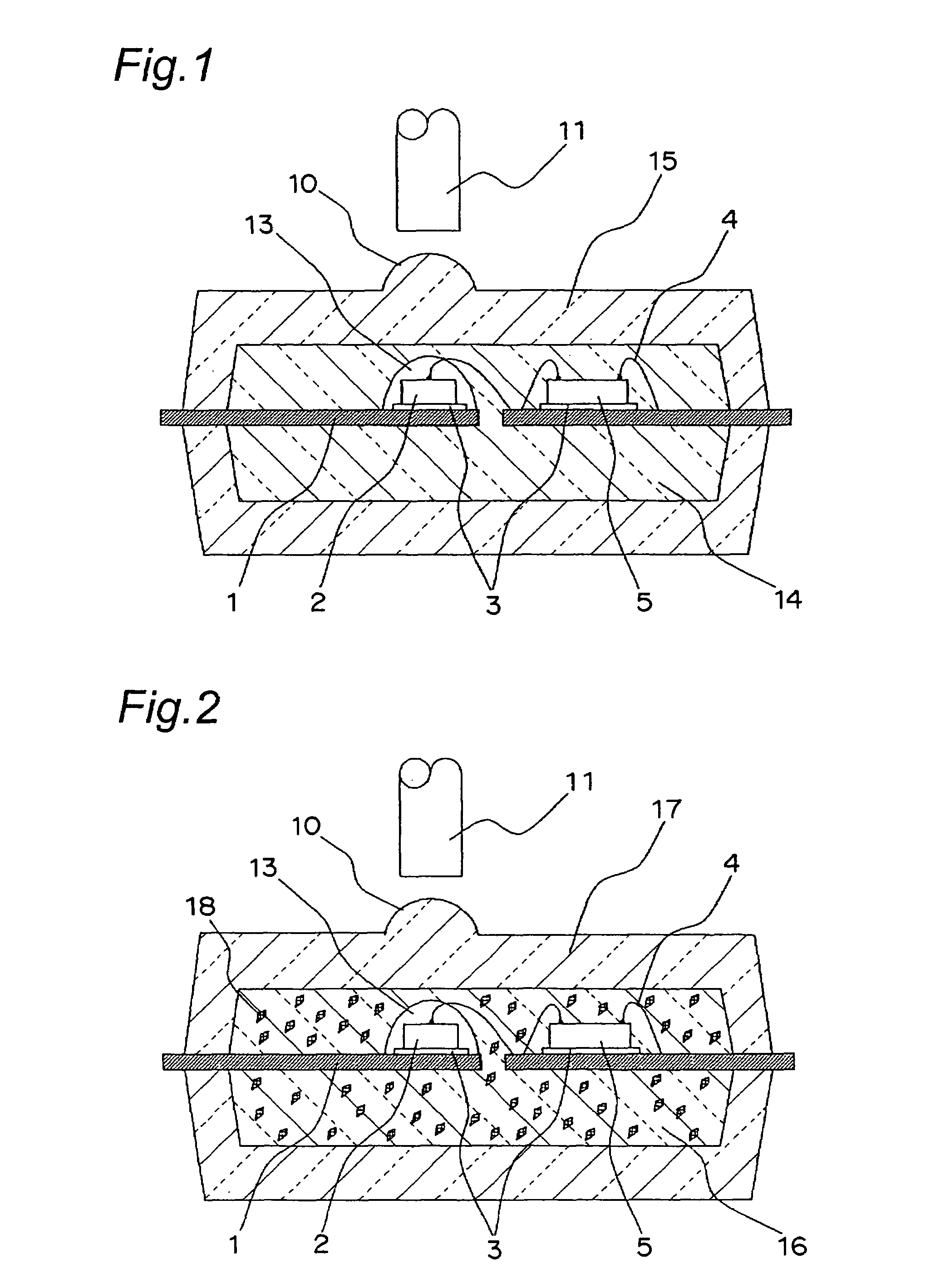
[0215]FIG. 6 is a schematic structural view of the optical semiconductor device of the ninth embodiment of the present invention. The optical semiconductor device of the ninth embodiment of the present invention has the same construction as that of the sixth embodiment except for the first mold resin portion, and like components are denoted by like reference numerals with no description provided therefor.

[0216]In the optical semiconductor device of the ninth embodiment, as shown in FIG. 6, an acid anhydride curing epoxy resin filled with transparent filler 18′ is used for the second mold resin portion 19. The loading weight of filler with which the second mold resin portion 19 is filled is set to 75% or less than that of the filler with which the first mold resin portion 21 is filled.

[0217]According to the optical semiconductor device of the ninth embodiment, an optical semiconductor device, which is able to reduce the difference in the coefficient of linear expansion between the fi...

tenth embodiment

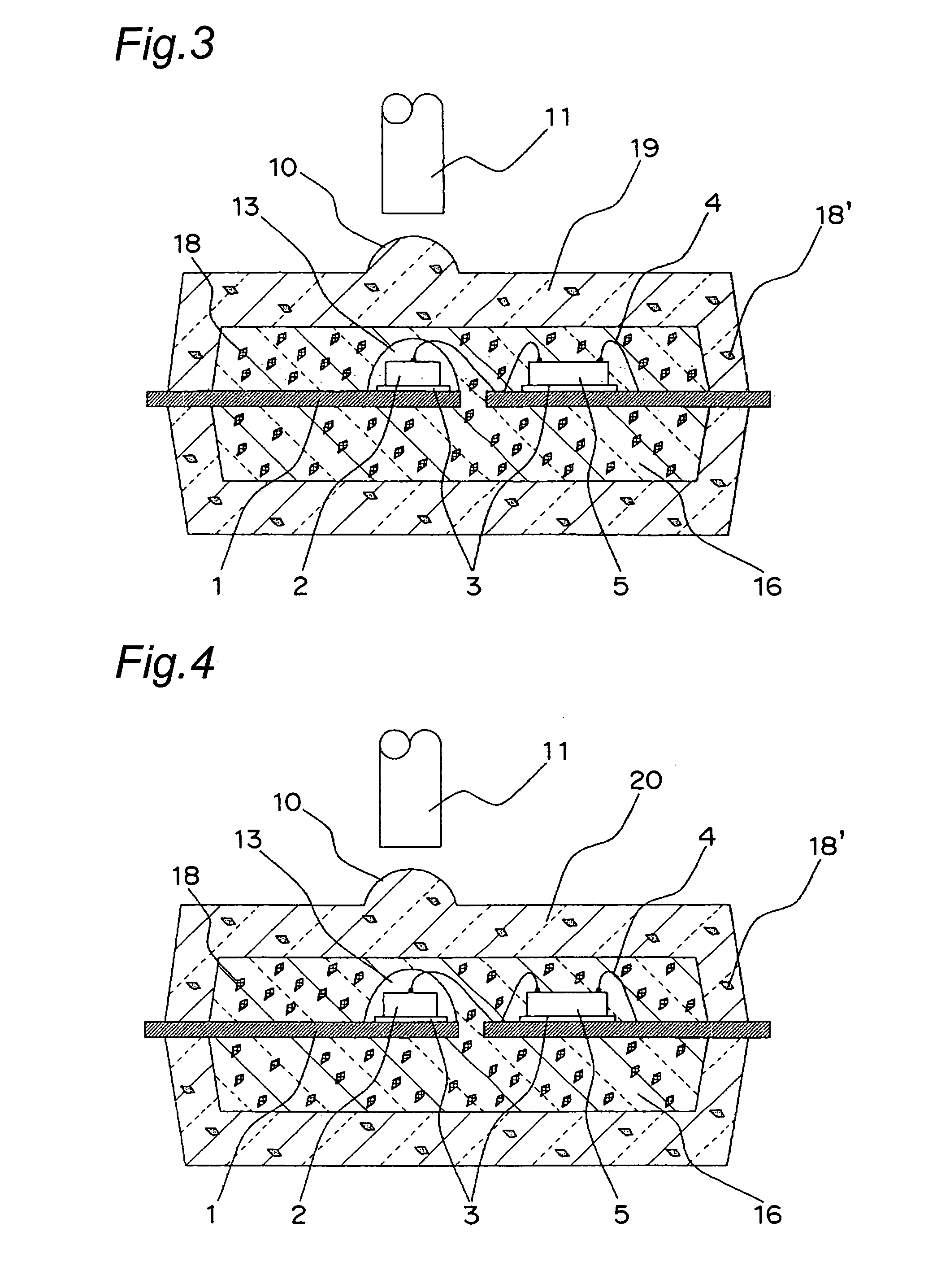
[0218]FIG. 7 is a schematic structural view of the optical semiconductor device of the tenth embodiment of the present invention. The optical semiconductor device of the tenth embodiment of the present invention has the same construction as that of the ninth embodiment except for the second mold resin portion, and like components are denoted by like reference numerals with no description provided therefor.

[0219]In the optical semiconductor device of the tenth embodiment, as shown in FIG. 6, a phenolic curing epoxy resin, of which the loading weight of the transparent filler 18′ is smaller than that of the first mold resin portion 21, is used for the second mold resin portion 20.

[0220]According to the optical semiconductor device of the tenth embodiment, the difference in the coefficient of linear expansion between the first mold resin portion 21 and the second mold resin portion 20 is reduced, and the occurrence of resin interface separation due to thermal stresses can be reduced by...

eleventh embodiment

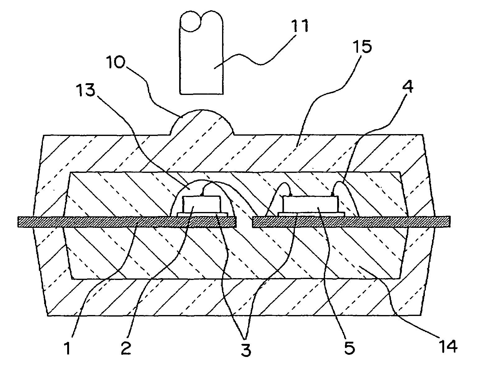
[0221]Next, the optical semiconductor device of the eleventh embodiment of the present invention has the same construction as that of the optical semiconductor device of the fifth embodiment except for the first mold resin portion and should correspondingly be referred to FIG. 2.

[0222]In the optical semiconductor device of the eleventh embodiment, the loading weight of the transparent filler with which the first mold resin portion 16 is filled is controlled within a range of 20 to 80 percent by weight.

[0223]According to the optical semiconductor device of the eleventh embodiment, an optical semiconductor device, which is able to reduce the coefficient of linear expansion α1 of the first mold resin portion 16, increase the thermal conductivity with a high transmissivity maintained and has a satisfactory optical transmission quality and a high reliability, can be fabricated compactly at low cost.

[0224]The condition of the loading weight of the transparent filler of the optical semicon...


PUM


Abstract

An optical semiconductor element 2 is mounted on a lead frame 1, the optical semiconductor element 2 is encapsulated with a mold resin portion 14 of a first layer that has light permeability, and the mold resin portion 14 of the first layer is encapsulated with a mold resin portion 15 of a second layer that has light permeability. Then, a coefficient of linear expansion of the mold resin portion 14 of the first layer is made smaller than a coefficient of linear expansion of the mold resin portion 15 of the second layer.

Description

[0001]This nonprovisional application claims priority under 35 U.S.C. §119(a) on Patent Application No. 2004-269470 filed in Japan on Sep. 16, 2004, patent application No. 2005-048556 filed in Japan on Feb. 24, 2005, patent application No. 2005-109735 filed in Japan on Apr. 6, 2005 and patent application No. 2005-213184 filed in Japan on Jul. 22, 2005, the entire contents of which are hereby incorporated by reference.BACKGROUND OF THE INVENTION[0002]The present invention relates to optical semiconductor devices that have optical semiconductor elements and relates, in particular, to an optical semiconductor device which can be utilized for an optical communication device that transmits and receives optical signals by means of an optical transmission medium of an optical fiber or the like.[0003]The optical semiconductor device of the present invention is used for electronic equipment such as digital TV (Television) sets, digital BS (Broadcasting Satellite) tuners, CS (Communication Sa...

Claims


Application Information

Patent Timeline
Patent Type & Authority Patents(United States)
IPC IPC(8): H01L21/00H01L33/56
CPCH01L21/565H01L23/3135H01L23/49575H01L24/48H01L24/97H01L25/167H01L24/45H01L33/56H01L2224/45144H01L2224/4809H01L2224/48091H01L2224/48095H01L2224/48247H01L2224/4846H01L2224/48465H01L2224/48471H01L2224/48479H01L2224/48599H01L2224/73265H01L2224/85051H01L2224/85986H01L2224/97H01L2924/01005H01L2924/01007H01L2924/01013H01L2924/01014H01L2924/01029H01L2924/01046H01L2924/01074H01L2924/01078H01L2924/01079H01L2924/01082H01L2924/14H01L2924/3025H01L2224/32245H01L2924/01006H01L2924/01019H01L2924/01033H01L2924/01055H01L2924/01068H01L2224/8592H01L2924/12041H01L2924/1815H01L2924/00014H01L2224/85186H01L2924/00H01L2924/00012H01L2224/48227H01L24/73H01L2924/12043H01L2924/181H01L2924/351H01L2224/4554H01L2224/85399H01L2224/05599
Inventor SHOJI, HIROYUKITAKAKURA, HIDEYAKUSUDA, KAZUO
Owner SHARP KK
Why Eureka
Try Eureka