Method for controlling thickness uniformity of electroplated layers

a technology of thickness uniformity and electroplating layer, which is applied in the direction of electrolysis components, manufacturing tools, cell components, etc., can solve the problems of high removal process cost, use of electrodeplating materials by electrical thieves, etc., and achieve the effect of increasing or decreasing the ra

Inactive Publication Date: 2008-10-14
NUVASIVE +1
View PDF56 Cites 11 Cited by
  • Summary
  • Abstract
  • Description
  • Claims
  • Application Information

AI Technical Summary

Benefits of technology

[0025]At least one control power source can be used to supply a voltage to at least one of the electrically isolated sections to vary the rate of conductive material deposition onto a region of the substrate surface. In one configuration, the rate can be increased or decreased. Apparatuses such as those mentioned can be used to control thickness uniformity during conductive material deposition in a process including contacting the anode with the electrolyte, providing a supply of the electrolyte to the substrate surface through the conductive element and through the mask lying over the conductive element, providing a potential between the anode and the surface, and supplying a voltage to the conductive element in order to vary the conductive material deposition rate.

Problems solved by technology

These removal processes are known to be quite costly.
Also, the resulting thickness uniformity of the plating process, i.e. the uniformity of thickness t3 in FIG. 1D and the uniformity of the thickness t5 in FIG. 1E, needs to be very good (typically less than 10% variation, and preferably less than 5% variation) because a non-uniform copper thickness causes problems during the CMP process.
Further, in such systems, electrical thieves can be used for electrodepositing materials.

Method used


Image

  • Method for controlling thickness uniformity of electroplated layers
  • Method for controlling thickness uniformity of electroplated layers
  • Method for controlling thickness uniformity of electroplated layers

Examples


Embodiment Construction

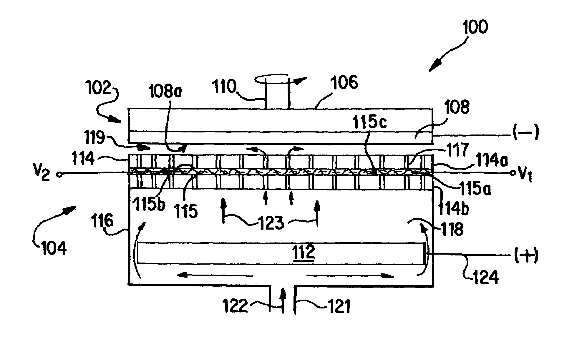
[0052]The present invention provides a method and a system to control the uniformity of a conductive material layer deposited on a surface of a semiconductor. The invention can be used with ECMD, mask pulse plating and full face plating as well as plating systems that deposit conformal films. The deposition process of the present invention advantageously achieves deposition of a conductive material in a plurality of cavities, such as trenches, vias, contact holes and the like, on a surface of a semiconductor wafer.

[0053]As is known, during an electrodeposition process of a surface of a wafer, the current density applied to the surface is substantially greater at the periphery of the surface than the center of the surface. In the prior art, this higher current density results in an increased deposition rate of the deposited film at the periphery of the wafer as compared to the wafer center. With the present invention, the film thickness difference between the interior and the periphe...


PUM

PropertyMeasurementUnit
aspect ratioaaaaaaaaaa
thicknessaaaaaaaaaa
conductiveaaaaaaaaaa

Abstract

An apparatus which can control thickness uniformity during deposition of conductive material from an electrolyte onto a surface of a semiconductor substrate is provided. The apparatus has an anode which can be contacted by the electrolyte during deposition of the conductive material, a cathode assembly including a carrier adapted to carry the substrate for movement during deposition, and a conductive element permitting electrolyte flow therethrough. A mask lies over the conductive element and has openings permitting electrolyte flow. The openings define active regions of the conductive element by which a rate of conductive material deposition onto the surface can be varied. A power source can provide a potential between the anode and the cathode assembly so as to produce the deposition. A deposition process is also disclosed, and uniform electroetching of conductive material on the semiconductor substrate surface can additionally be performed.

Description

[0001]This application is a continuation of U.S. patent application Ser. No. 09 / 855,059, filed May 15, 2001, now U.S. Pat. No. 6,802,946, which claims the priority of U.S. provisional application No. 60 / 256,924, filed Dec. 21, 2000, the disclosures of which are expressly incorporated by reference herein.BACKGROUND OF THE INVENTION[0002]1. Field of the Invention[0003]The present invention generally relates to electrodeposition process technology and, more particularly, to an electrodeposition process and apparatus that yield planar deposition layers.[0004]2. Description of Related Art[0005]A conventional semiconductor device generally includes a semiconductor substrate, usually a silicon substrate, and a plurality of sequentially formed dielectric interlayers, such as silicon dioxide interlayers, and conductive paths or interconnects made of conductive materials. The interconnects are usually formed by filling a conductive material in trenches etched into the dielectric interlayers. ...

Claims


Application Information

Patent Timeline
Patent Type & Authority Patents(United States)
IPC IPC(8): C25D5/04C25D5/22C25D7/12C25F3/16C25D17/00C25D17/10C25D21/00C25D21/12C25F7/00H01L21/288H01L21/768
CPCH01L21/2885H01L21/76877C25D7/123C25D17/001Y10S204/07C25F7/00C25D17/00
Inventor BASOL, BULENT M.LINDQUIST, PAUL
Owner NUVASIVE
Why Eureka
Try Eureka