
Diffractive optical element

a technology of optical elements and optical elements, applied in the field of diffractive optical elements, can solve the problems of not many kinds of high-power lasers, and the reduction of the pitch of boring holes requires enlargement of unit patterns, so as to accelerate and reduce the cost of laser processing, the effect of free, precise laser simultaneous multi-point processing

Active Publication Date: 2008-10-21
SUMITOMO ELECTRIC IND LTD
View PDF8 Cites 5 Cited by
  • Summary
  • Abstract
  • Description
  • Claims
  • Application Information

AI Technical Summary

Benefits of technology

This approach enables high-precision, multipoint laser processing at arbitrary points, enhancing the utility of DOEs in microprocessing and reducing the cost and acceleration of laser processing, while allowing for the production of non-regular, non-lattice point distributions, which is essential for electronic devices.

Problems solved by technology

However, we have not many kinds of high-power laser.
Thus, reduction of the pitch of boring holes requires enlargement of unit patterns.

Method used


Image

  • Diffractive optical element
  • Diffractive optical element
  • Diffractive optical element

Examples


embodiment 1

DOE of Embodiment 1

[0135]Diffraction rate: 82.2%[0136]Intensity fluctuation: 1.6%[0137]Largest noise intensity: 3.6%

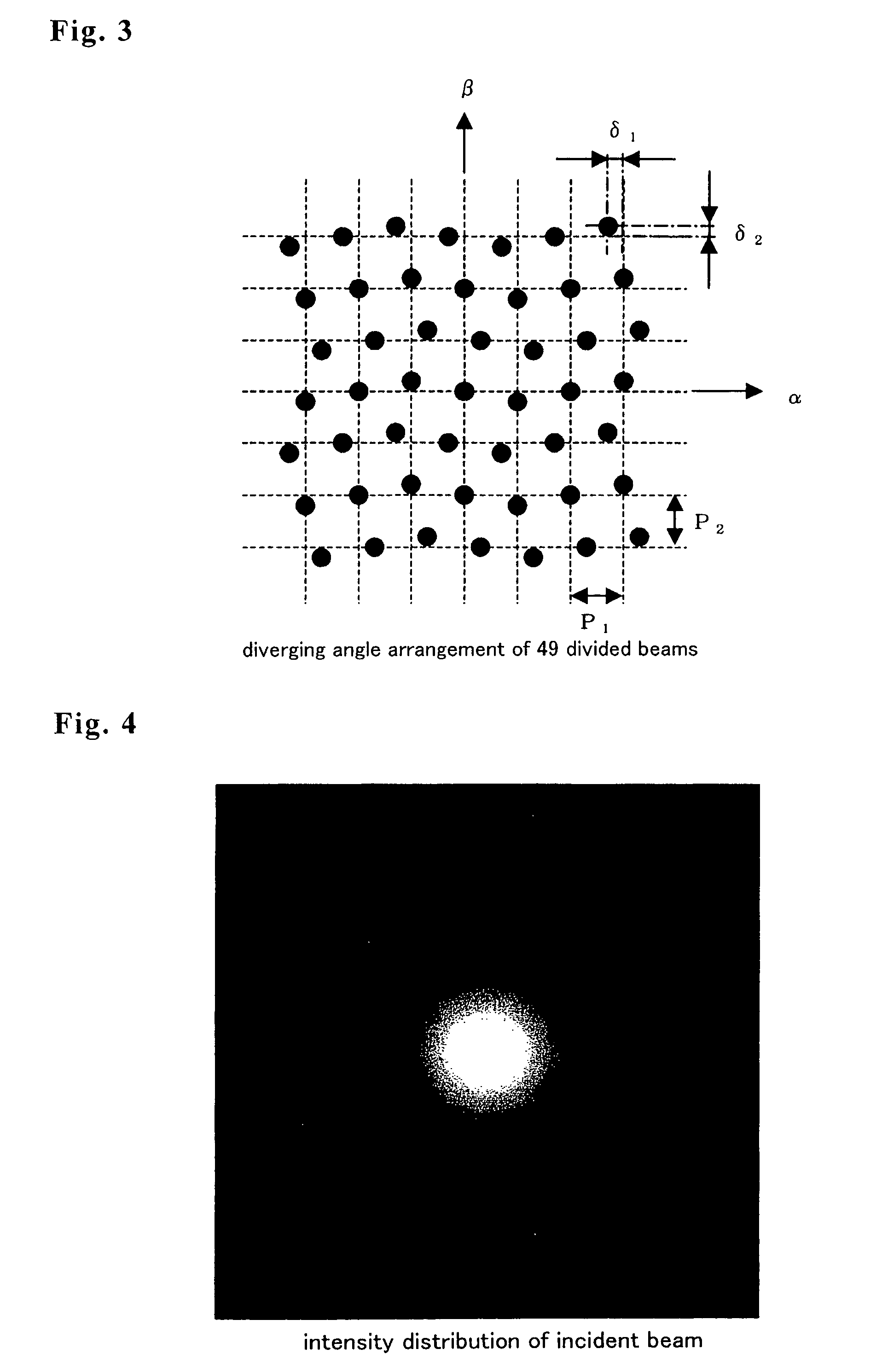
[0138]FIG. 4 is an incident beam intensity pattern. FIG. 5 is a DOE step distribution pattern. FIG. 6 is an image spot distribution pattern.

[C. Laser Processing Apparatus]

[0139]A laser processing apparatus is manufactured by combining a CO2 laser, the above-mentioned Fourier type DOE and a flat / convex lens (f=127 mm, 50.8 mm diameter, ZnSe). The spot diameter on an image plane is 171 μmφ.

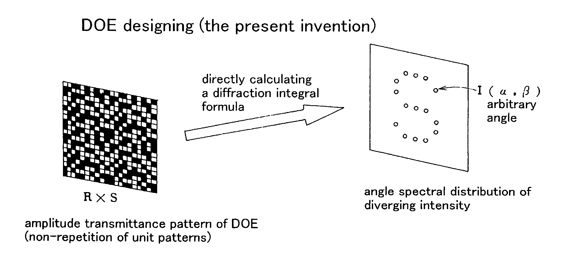
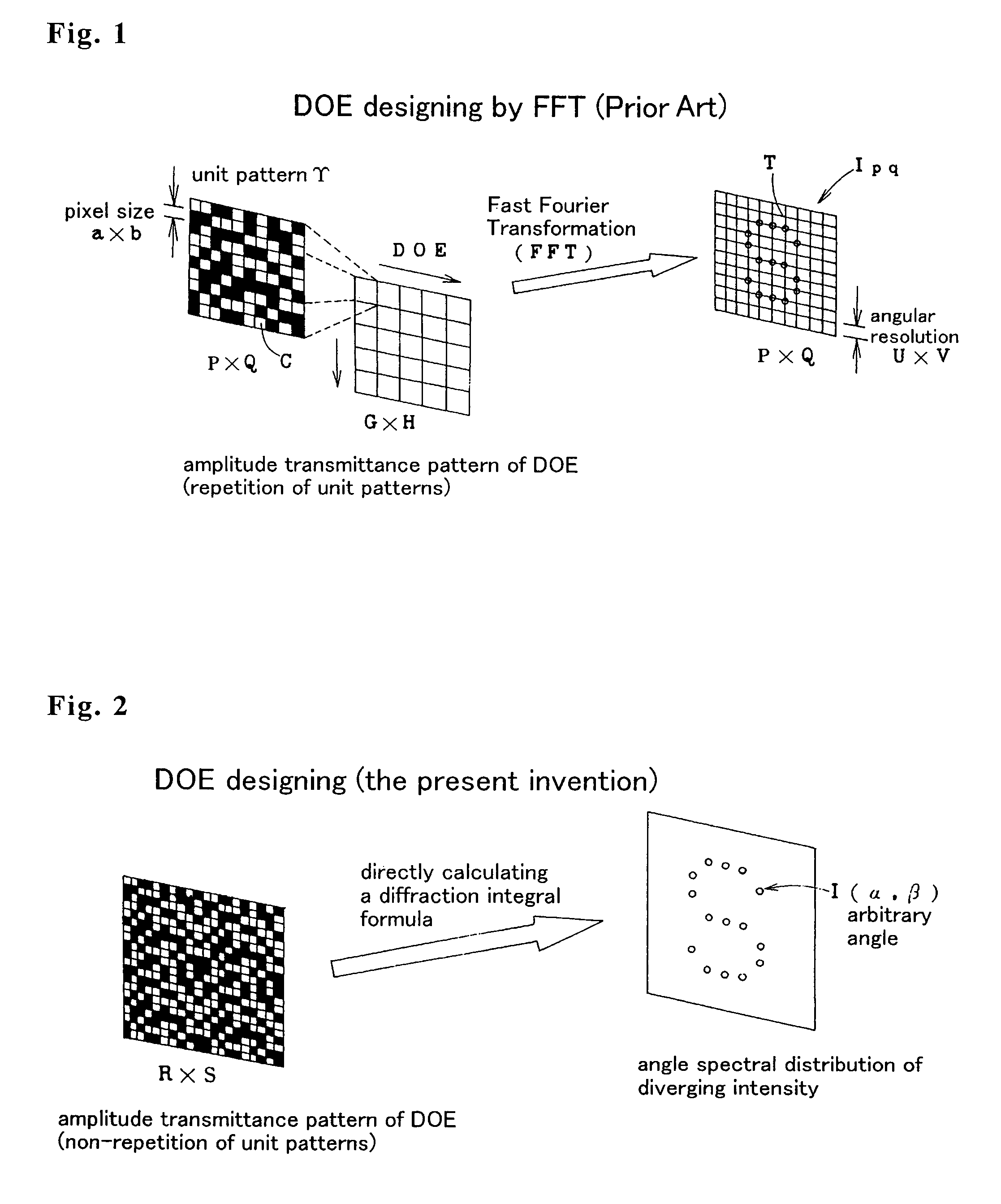
[0140]An object arrangement of spots in angular space of Embodiment 1 is shown in FIG. 3. The abscissa is a horizontal angle α. The ordinate is a vertical angle β. It should be noted that this pattern is not an image pattern projected onto the image plane. 7×7 spots align in α- and β-directions. The beam spots are not all upon lattice points but slightly deviate from the lattice points.

[0141]Four (±2, ±2) points, four (0, ±2), (±2, 0) points and one (0, 0) point are on the lattice poin...

embodiment 2

DOE of Embodiment 2

[0161]Diffraction rate: 71.6%[0162]Intensity fluctuation: 1.7%[0163]Largest noise intensity: 3.5%

[0164]The pattern of the DOE is depicted by FIG. 7. Thickness (height) distribution (16 steps) of the DOE is represented by a black-white monochromatic tone. FIG. 7 shows a lattice-like pattern with narrow lattice constants. A fine structure of tones within lattices are obscure. The DOE (FIG. 7) of Embodiment 2 is entirely different from the former DOE (FIG. 5) of Embodiment 1. Since the branching beam angles are large, repetition of the DOE pattern is fine in Embodiment 2.

[0165]No unit pattern should exist in the DOE in FIG. 7. There should be no repetition of unit patterns having the same shape and the same size. But, the DOE seems to have quasi-regular repetition of spots in two dimensions like cloth. It may be marvelous. But, the deviations δ1 and δ2 are quite small in comparison to the pitches P1 and P2 in Embodiment 1. Then, the DOE becomes similar to the convent...

embodiment 3

[Embodiment 3 (Fresnel Type DOE, Small Diverging Angles)]

[A. Properties of the Fresnel DOE]

[0168]Wavelength: 10.6 μm[0169]Mode: TEMoo [0170]Beam diameter (1 / e2): 10 mm[0171]Step number of heights: 16[0172]Pixel size: a=20 μm, b=20 μm[0173]Pixel number: R=1000 pixels, S=1000 pixels[0174]DOE size: aR=20 mm, bS=20 mm[0175]Number of divided beams: 49 (=7×7)[0176]Diffracted beam pattern: FIG. 3, P1=3.93701 mrad, P2=3.93701 mrad,

δ1=0.15748 mrad, δ2=0.07874 mrad[0177]Fresnel type lens: focal length f=−500 mm

[0178]What is different from Embodiment 1 (Fraunhofer type) is that the DOE has a function as a lens. Since the DOE has the lens function, the DOE is called as Fresnel type. Embodiment 3 adds an f=−500 mm concave lens to the DOE. Of course, a convex lens can be added to the DOE instead of the concave lens.

[0179]Necessary resolutions U and V in x- and y-directions are

U=δ1=0.15748 mrad,

V=δ2=0.07874 mrad.

[0180]In Embodiment 3, λ / aR=λ / bS=0.53 mrad like Embodiment 1. These values of paramete...


PUM

PropertyMeasurementUnit
diameteraaaaaaaaaa
diameteraaaaaaaaaa
sizeaaaaaaaaaa

Abstract

A conventional diffractive optical element (DOE), which consists of repetition of a unit pattern , has an advantage of applicability of the Fast Fourier Transform algorithm to calculate diffraction beam spots intensities on lattice points on an image plane. But, the conventional DOE has a drawback of impossibility of diffracting a laser beam off the lattice points. This invention designs a DOE by giving arbitrary complex amplitude transmittance {tmn} to every pixel (m, n), calculating actual Fourier transform from {tmn} to intensity W(alpha, beta), and obtaining intensity of a diffraction beam directing in any alpha and beta direction. Since alpha, beta are not necessary to be on lattice points, the FFT is of no use. Angular resolutions U and V satisfy inequalities U<lambda / aR and V<lambda / bS, where lambda is a wavelength, aR and bS are the size of the DOE. The DOE can produce multidiffracted beams anywhere on an image and can irradiate a plurality of arbitrary arranged points simultaneously with high precision. The DOE realizes precise multispot microprocessing on arbitrary positions, which is required for producing electronic parts. The DOE is suitable for high speed and low cost laser processing.

Description

TECHNICAL FIELD[0001]This invention relates to a diffractive optical element allowing a laser beam to branch into a plurality of beams and to shoot at any spots deviating from lattice points regularly assigned to an image plane and a laser machining apparatus using the same diffractive optical element, particularly, a multipoint batch laser processing apparatus used for microprocessing of electronic parts, such as perforating, welding, soldering or surface treatment.BACKGROUND ART[Patent Reference Document 1] Japanese Patent Publication No.2000-231012, “Method for Designing a Diffractive Optical Element”[0002]This is one of the former inventions made by the inventor of the present invention. The application proposed a diffractive optical elements (DOE: Fraunhofer type) having functions of dividing a laser beam. The invention aimed at facilitating the designing of DOEs by assigning inherently narrow tolerance parameters with larger tolerances enlarged by the estimating designed DOEs ...

Claims


Application Information

Patent Timeline
Patent Type & Authority Patents(United States)
IPC IPC(8): G02B5/18G02B27/46
CPCB23K26/0656G02B27/1086G02B27/12B23K26/066G02B5/1814G02B27/46
Inventor FUSE, KEIJI
Owner SUMITOMO ELECTRIC IND LTD
Learn More