Control of memory devices possessing variable resistance characteristics

a memory device and resistance characteristic technology, applied in the field of memory devices, can solve the problems of volatile memory devices losing information, increasing the volume, use and complexity of computers and electronic devices, and increasing the complexity of volatile memory devices, so as to facilitate data storage, increase the accuracy and efficiency of programming multi-bit memory devices, and inherent variability of internal resistance of memory devices

Active Publication Date: 2008-10-28
CYPRESS SEMICON CORP
View PDF12 Cites 17 Cited by
  • Summary
  • Abstract
  • Description
  • Claims
  • Application Information

AI Technical Summary

Benefits of technology

[0015]Apparatus and methods are provided for facilitating programming and erasing organic and / or inorganic memory devices. The present invention utilizes a means that allows control of the inherent variability of the internal resistance of a memory device during programming and erasing. The present invention provides increased accuracy and efficiency in programming multi-bit memory devices.
[0016]The present invention additionally facilitates data storage by aiding the efficiency in the way memory devices change states. By utilizing constant current sources, the memory can accurately be programmed into one of the numerous states available to the memory. This allows for quick and precise programming of the multi-bit devices without memory damaging current spikes. Likewise, by utilizing constant voltage sources, the memory can be erased independent of large dynamic resistance changes inherent some types of memory. The present invention also allows for efficient manufacturing of higher quality memory devices by employing constant current and voltage sources, reducing malfunctions and increasing reliability.

Problems solved by technology

The volume, use and complexity of computers and electronic devices are continually increasing.
The long term storage mediums typically store larger amounts of information at a lower cost, but are slower than other types of storage devices.
Volatile memory devices generally lose their information if they lose power and typically require periodic refresh cycles to maintain their information.
However, silicon-based devices are approaching their fundamental physical size limits.
Inorganic solid state devices are generally encumbered with a complex architecture which leads to high cost and a loss of data storage density.
The volatile semiconductor memories based on inorganic semiconductor material must constantly be supplied with electric current with a resulting heating and high electric power consumption in order to maintain stored information.
Non-volatile semiconductor devices have a reduced data rate and relatively high power consumption and large degree of complexity.
Moreover, as the size of inorganic solid state devices decreases and integration increases, sensitivity to alignment tolerances increases making fabrication markedly more difficult.
Scaling inorganic solid state devices raises issues with dopant diffusion lengths.
As dimensions are reduced, the dopant diffusion lengths in silicon are posing difficulties in process design.
However, it is not clear that such accommodations can be continued indefinitely.
However, if the voltage change per unit distance is large, further difficulties are created in that a large voltage change per unit distance implies that the magnitude of the electric field is large.
Such an electron is known as a hot electron, and may be sufficiently energetic to pass through an insulator, leading to irreversibly degradation of a semiconductor device.
Scaling and integration makes isolation in a monolithic semiconductor substrate more challenging.
In particular, lateral isolation of devices from each other is difficult in some situations.
Another difficulty is leakage current scaling.
Yet another difficulty is presented by the diffusion of carriers within the substrate; that is free carriers can diffuse over many tens of microns and neutralize a stored charge.
Thus, further device shrinking and density increasing may be limited for inorganic memory devices.
Furthermore, such device shrinkage for inorganic non-volatile memory devices while meeting increased performance demands is particularly difficult, especially while maintaining low costs.

Method used


Image

  • Control of memory devices possessing variable resistance characteristics
  • Control of memory devices possessing variable resistance characteristics
  • Control of memory devices possessing variable resistance characteristics

Examples


Embodiment Construction

[0030]The following is a detailed description of the present invention made in conjunction with the attached figures, wherein like reference numerals will refer to like elements throughout.

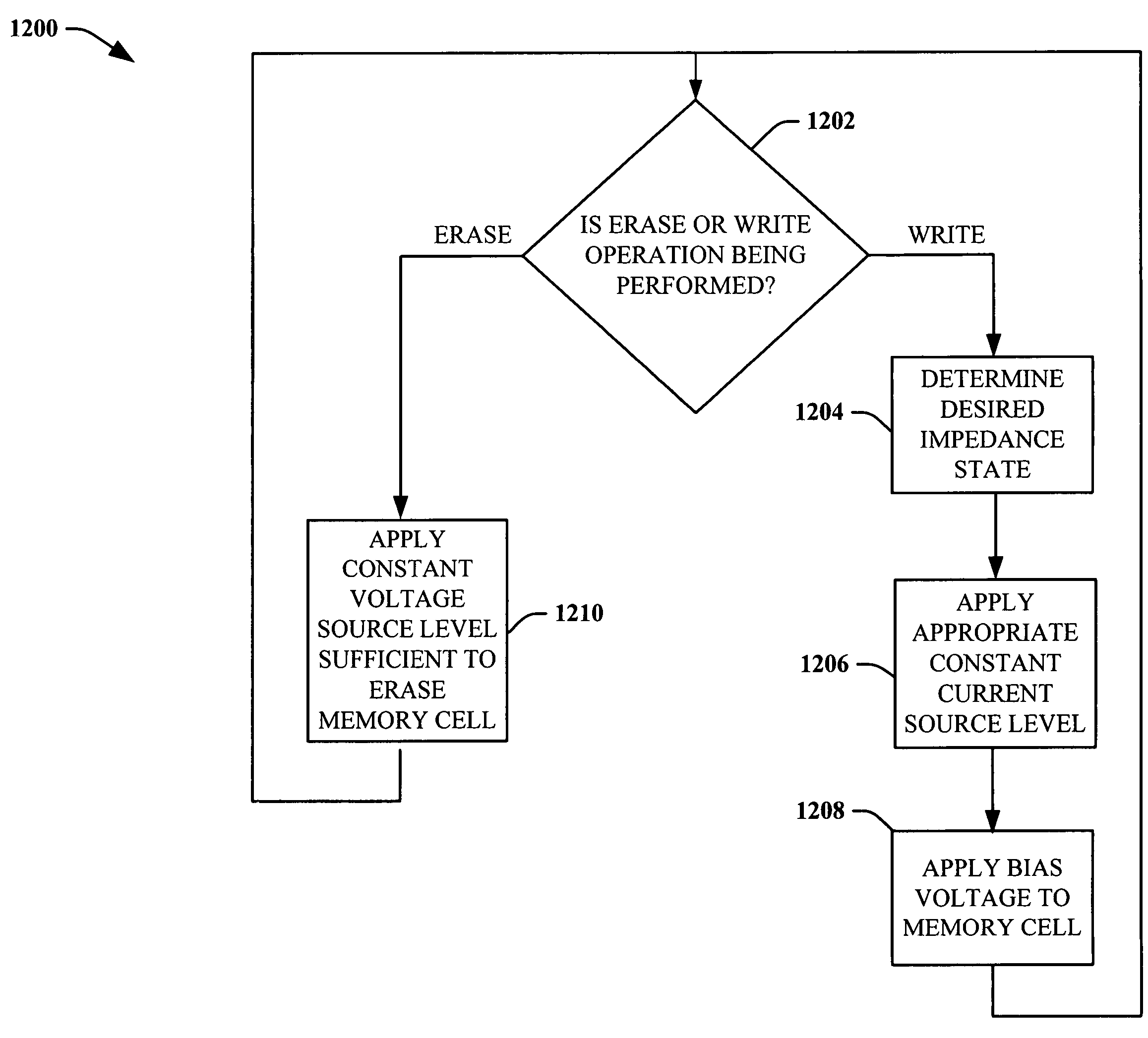
[0031]Cells of a memory device are generally operative to be of two or more states corresponding to various levels of impedance. These states are set by applying a bias voltage and then the cells remain in their respective states until another voltage, in reverse bias, is applied. The cells maintain their states with or without power (e.g., non-volatile) and can be read either electrically or optically by measuring injection current or light emission. The systems and methods of the present invention facilitate both the programming (writing) and erasing of memory devices via control of their resistance characteristics.

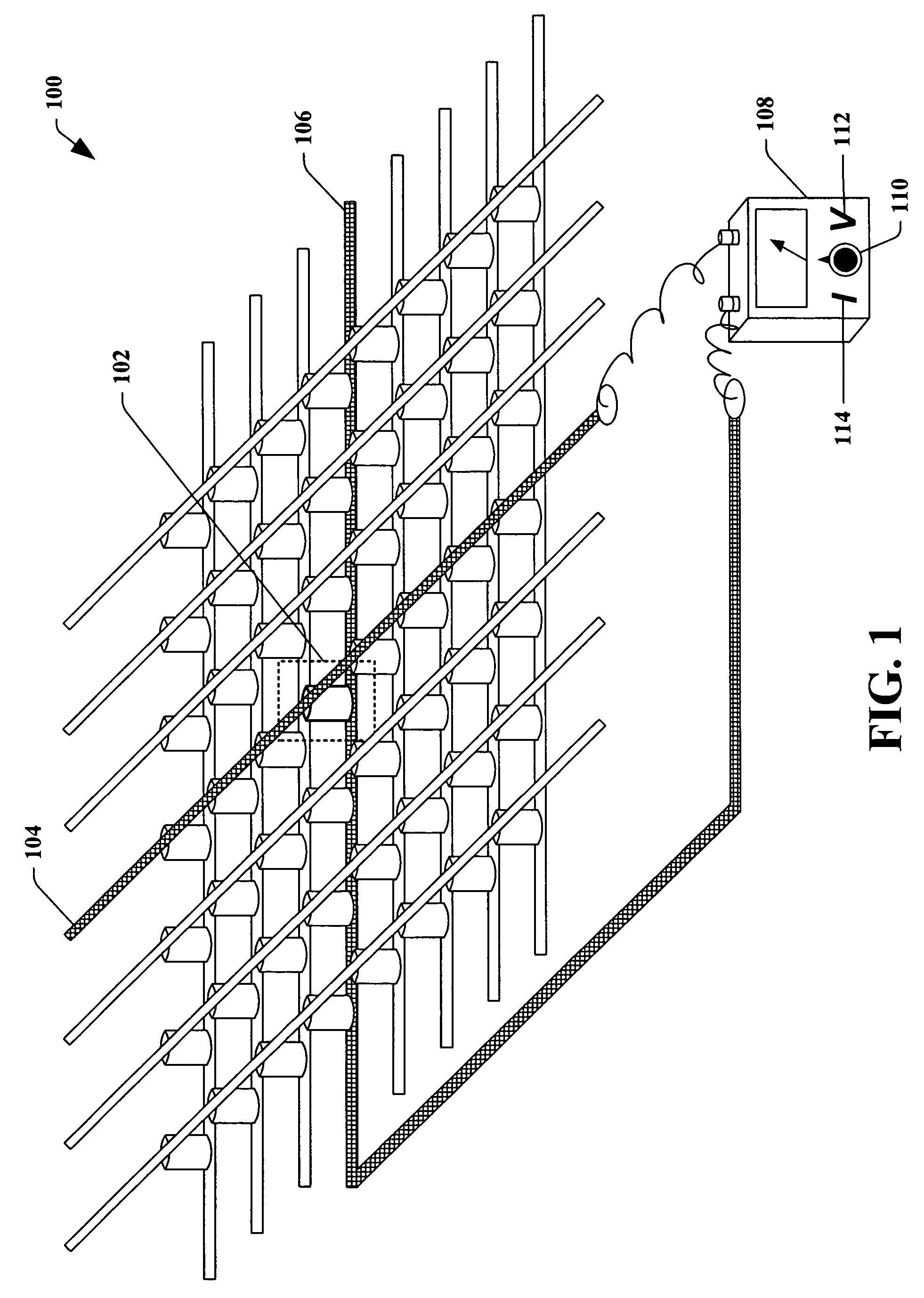
[0032]In FIG. 1, a three dimensional diagram of a memory device array 100 in accordance with an aspect of the present invention is illustrated. FIG. 1 is a notional example depicting ...


PUM


Abstract

Systems and methods employing at least one constant current source to facilitate programming of an organic memory cell and / or employing at least one constant voltage source to facilitate erasing of a memory device. The present invention is utilized in single memory cell devices and memory cell arrays. Employing a constant current source prevents current spikes during programming and allows accurate control of a memory cell's state during write cycles, independent of the cell's resistance. Employing a constant voltage source provides a stable load for memory cells during erase cycles and allows for accurate voltage control across the memory cell despite large dynamic changes in cell resistance during the process.

Description

REFERENCE TO RELATED APPLICATIONS[0001]This is a continuation application of U.S. patent application Ser. No. 10 / 951,375, filed Sep. 28, 2004, entitled, “CONTROL OF MEMORY DEVICES POSSESSING VARIABLE RESISTANCE CHARACTERISTICS”. The entirety of this application is incorporated herein by reference.FIELD OF INVENTION[0002]The present invention relates generally to memory devices and, in particular, to controlling resistance characteristics of memory devices for erasing and programming.BACKGROUND OF THE INVENTION[0003]The volume, use and complexity of computers and electronic devices are continually increasing. Computers consistently become more powerful through new and improved electronic devices that are being continuously developed (e.g., digital audio players, video players). Additionally, the growth and use of digital media (e.g., digital audio, video, images, and the like) have further pushed the development of these devices. Such growth and development has vastly increased the a...

Claims


Application Information

Patent Timeline
Patent Type & Authority Patents(United States)
IPC IPC(8): G11C11/00
CPCB82Y10/00G11C11/5664G11C13/0014G11C13/0069G11C13/0097G11C2013/0071G11C2013/0078G11C2213/15G11C2213/79G11C16/06G11C16/02H10K19/00G11C16/14G11C16/12G11C16/10G11C16/16
Inventor FANG, TZU-NINGVAN BUSKIRK, MICHAEL ALLENBILL, COLIN S.
Owner CYPRESS SEMICON CORP
Why Eureka
Try Eureka