Electronic device, magnetoresistance effect element; magnetic head, recording/reproducing apparatus, memory element and manufacturing method for electronic device

a technology of magnetoresistance and effect, which is applied in the field of electromechanical devices and magnetoresistance effect elements, can solve the problems of insufficient memory elements, difficult to apply elements to fine structured magnetic heads, and low mr ratio of magnetic resistance memory using tmr film, etc., and achieves stable conductivity, reduced contact resistance between the first electrode and the second electrode, and free from variation in conductivity

Inactive Publication Date: 2008-11-11
PANASONIC CORP
View PDF9 Cites 1 Cited by
  • Summary
  • Abstract
  • Description
  • Claims
  • Application Information

AI Technical Summary

Benefits of technology

[0036]The second electronic device of the present invention includes a first electrode and a second electrode; and a metal conductor that bridges a gap between the first electrode and the second electrode. The bridge length L of the metal conductor portion is not more than a mean free path Λ of electron in the metal conductor at the operation temperature of the electronic device. The electronic device is manufactured by: forming the first electrode and the second electrode on a substrate with a gap having the bridge length L; forming a support that includes at least one selected from the group consisting of a nano-tube and a nano-wire and bridges a gap between the first electrode and the second electrode; and depositing the metal conductor on the support.
[0037]In the second electronic device of the present invention, the first electrode and the second electrode are formed on the substrate with a gap having the bridge length L; the support that includes at least one selected from the group consisting of a nano-tube and a nano-wire and bridges a gap between the first electrode and the second electrode is formed; and the metal conductor is deposited on the support. It is possible to form the metal conductor that has the bridge length L that is not more than the mean free path Λ of electron and directly bridges the first electrode and the second electrode on the support that includes at least one selected from the group consisting of the nano-tube and the nano-wire and directly bridges between the first electrode and the second electrode.
[0038]In the second electronic device of the present invention, similar to the first electronic device of the present invention, in the metal conductor, a phenomenon called quantum conductance appears. The metal conductor is different from the carbon nano-tube described in the non-patent document 4 and has a stable conductivity. Furthermore, the contact resistance to the first electrode and the second electrode is reduced. Therefore, by using the quantum conductance, by controlling the cross sectional area of the metal conductor portion, an electronic device free from variation in conductivity can be obtained.
[0039]The third electronic device of the present invention includes a first electrode film; an insulating film formed on the first electrode film; a second electrode film formed on the insulating film; and a metal con

Problems solved by technology

Therefore, it is difficult to apply the element to the fine structured magnetic head.
However, the MR ratio of the magnetic resistance memory using the TMR film is about 50%, which is insufficient as a memory element.
In a conventional lithography technology, it is extremely difficult to form a fine shape controlled on the order of nanometers.
However, the conductivity of the carbon nano-tube differs depending upon the chirality, so that it is difficult to control the formed carbon nano-tube becoming an arm-chair type exhibiting a property of metal property or a zigzag type exhibiting a property of a semiconductor or a chiral type exhibiting

Method used


Image

  • Electronic device, magnetoresistance effect element; magnetic head, recording/reproducing apparatus, memory element and manufacturing method for electronic device
  • Electronic device, magnetoresistance effect element; magnetic head, recording/reproducing apparatus, memory element and manufacturing method for electronic device
  • Electronic device, magnetoresistance effect element; magnetic head, recording/reproducing apparatus, memory element and manufacturing method for electronic device

Examples


embodiment 1

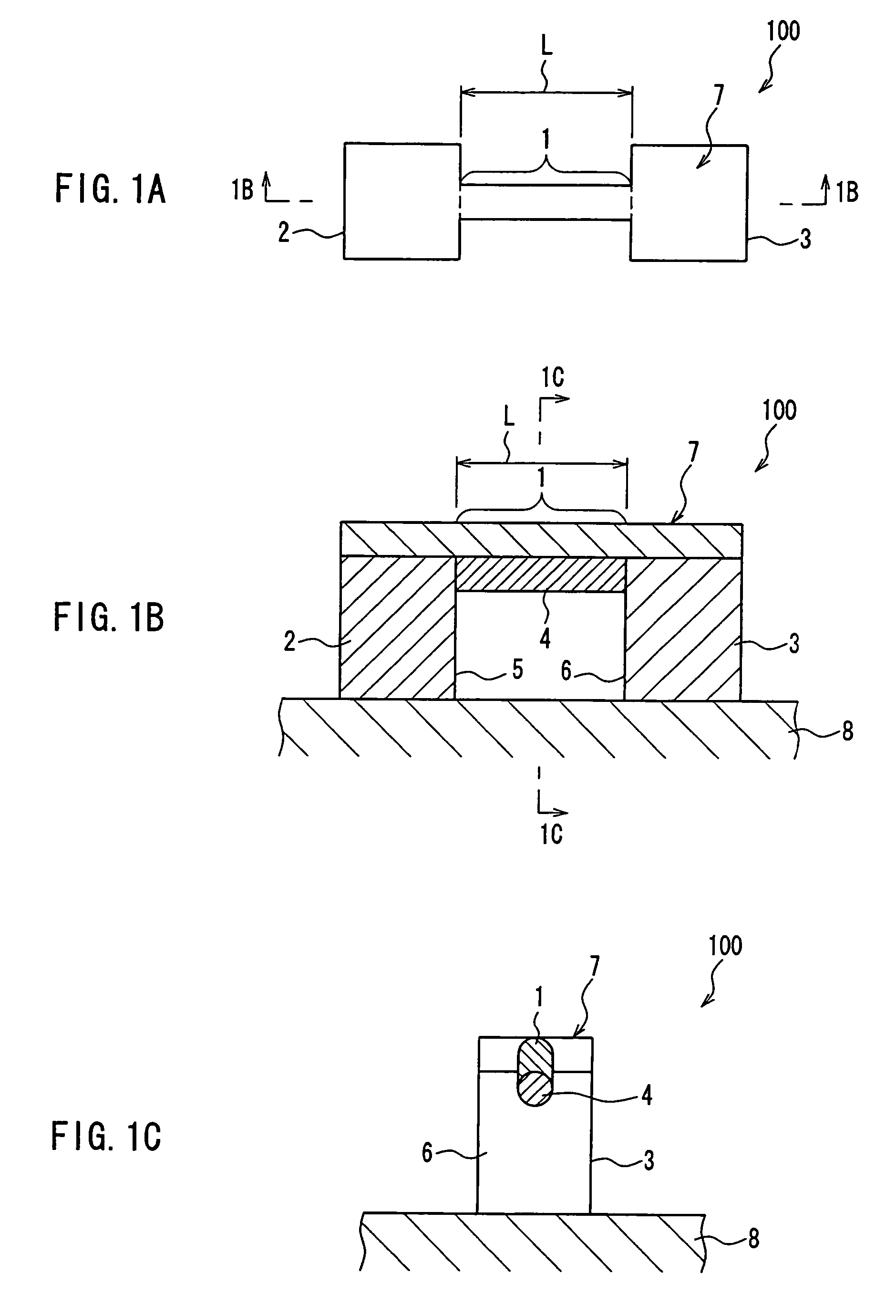
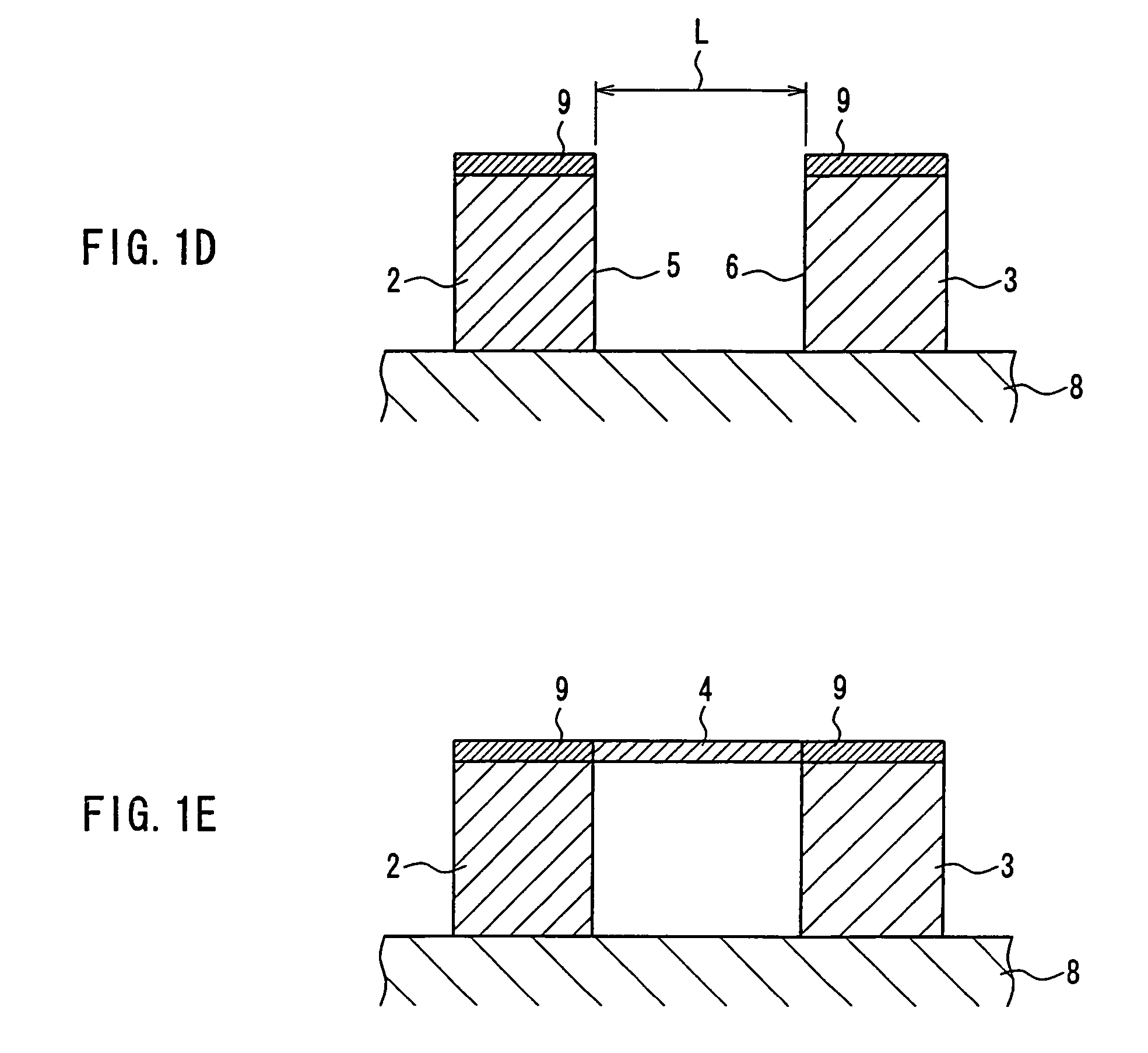
[0139]FIG. 1A is a plan view showing an electronic device 100 according to Embodiment 1; FIG. 1B is a cross-sectional view taken along a line 1B-1B in FIG. 1A; and FIG. 1C is a cross-sectional view taken along a line 1C-1C in FIG. 1B.

[0140]The electronic device 100 has rectangular parallelepiped shaped electrodes 2 and 3 formed on a substrate 8. The electrodes 2 and 3 have opposing surfaces 5 and 6 that are opposed to each other, respectively. Materials for the electrodes 2 and 3 are desirably metal or alloy.

[0141]The electronic device 100 is provided with a cylindrical support 4 including a carbon nano-tube for bridging the opposing surface 5 of the electrode 2 and the opposing surface 6 of the electrode 3. The carbon nano-tube may be a single layer carbon nano-tube (SWCNT) or may be a multiple layer carbon nano-tube (MWCNT).

[0142]The electronic device 100 has a metal conductor thin film 7 that is electrically connected to the electrodes 2 and 3. The metal conductor thin film 7 inc...

embodiment 2

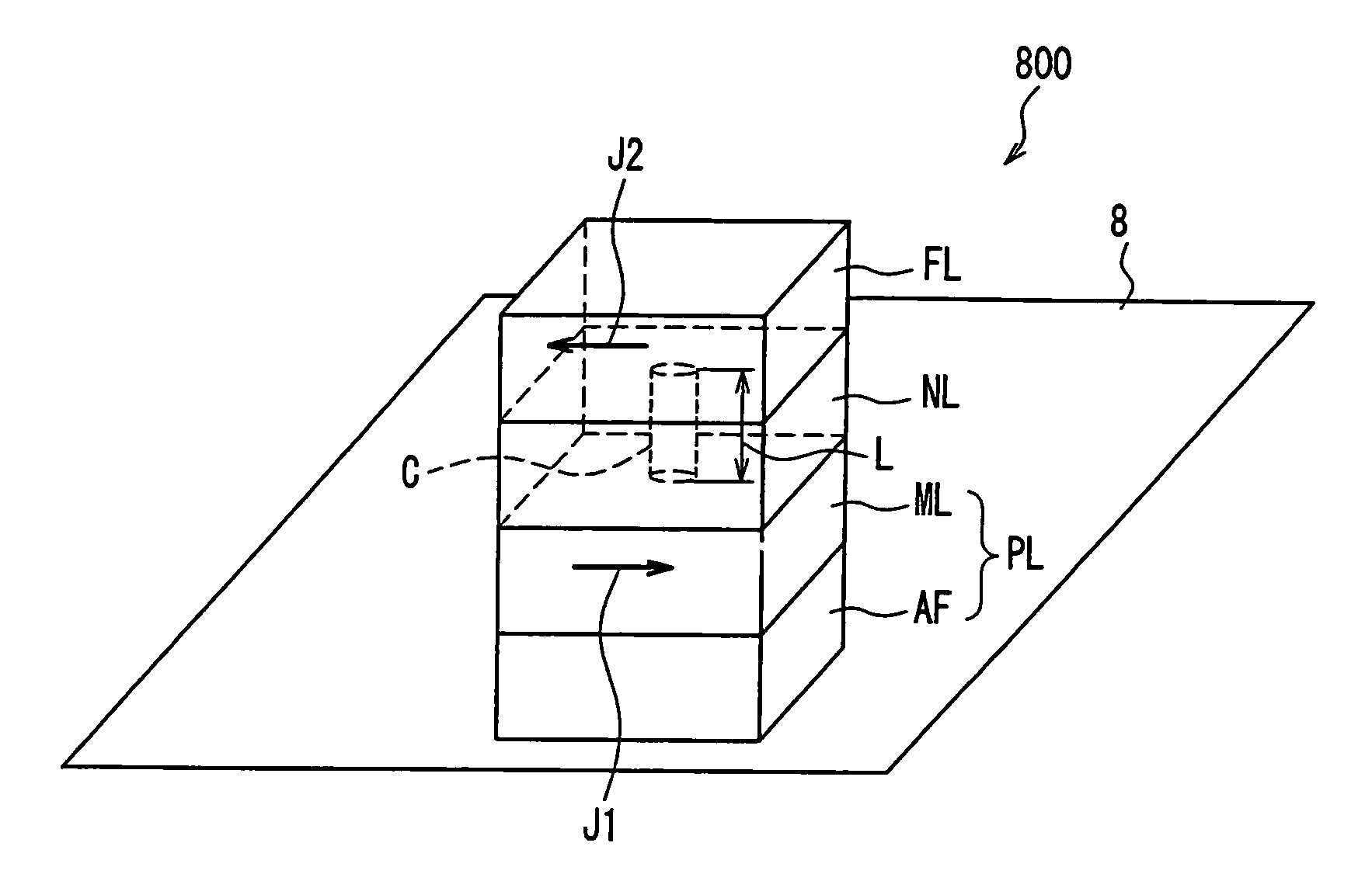
[0195]FIG. 4A is a plan view showing a magnetoresistance effect element 200 according to Embodiment 2; FIG. 4B is a front view thereof, and FIG. 4C is a cross-sectional view taken along a line 4C-4C of FIG. 4B. The same components as those mentioned in Embodiment 1 are denoted with the same reference numerals, and the repeated description may be omitted.

[0196]The magnetoresistance effect element 200 includes electrodes 2E and 3E made of a magnetic substance. The electrodes 2E and 3E respectively have the opposing surfaces 5E and 6E opposing each other. The electrodes 2E and 3E include a curved portion having a width D that is reduced to the width d respectively toward the opposing surfaces 5E and 6E.

[0197]The magnetoresistance effect element 200 is provided with a cylindrical support 4E made of a carbon nano-tube that bridges the opposing surface 5E of the electrode 2E and the opposing surface 6E of the electrode 3E.

[0198]The magnetoresistance effect element 200 has a metal conducto...

embodiment 3

[0211]FIG. 5A is a plan view showing a magnetic head 300 according to Embodiment 3; and FIG. 5B is a front view thereof. The same components mentioned in Embodiments 1 and 2 are denoted with the same reference numerals, and the repeated description may be omitted.

[0212]The magnetic head 300 includes a magnetoresistance effect element 200A. The magnetoresistance effect element 200A includes the electrodes 2F and 3F composed of a magnetic substance. The electrodes 2F and 3F have the opposing surfaces 5F and 6F, respectively. The electrodes 2F and 3F include a curved portion having a width D that decreases toward the width d of the opposing surfaces 5F and 6F, respectively.

[0213]The magnetoresistance effect element 200A is provided with a cylindrical support 4F made of carbon nano-tube that bridges between the opposing surface 5F of the electrodes 2F and the opposing surface 6F of the electrodes 3F

[0214]The magnetoresistance effect element 200A has a metal conductor thin film 7F electr...


PUM


Abstract

An electronic device free from variation of conductivity is provided. The electronic device 100 includes electrodes 2 and 3; and a metal conductor thin film 7 electrically connected to the electrodes 2 and 3. The metal conductor thin film 7 includes a metal conductor portion 1 that bridges a gap between the electrodes 2 and 3. The bridge length L of the metal conductor portion 1 is not more than a mean free path Λ of electron in the metal conductor portion 1 at the operation temperature of the electronic device 1. The electronic device 100 is formed by forming the electrodes 2 and 3 on the substrate 8 with a gap having the bridge length L; forming a support 4 that includes at least one selected from the group consisting of a nano-tube and a nano-wire and bridges a gap between the electrodes 2 and 3; and forming the metal conductor portion 1 by depositing the metal conductor thin film 7 on the support 4, and the electrodes 2 and 3.

Description

[0001]This application is a Non-Provisional application of Ser. No. 60 / 491,921, filed Aug. 1, 2003, which application is incorporated herein by reference.BACKGROUND OF THE INVENTION[0002]1. Field of the Invention[0003]The present invention relates to an electronic device having a fine shape controlled in the nanometer order, a magnetoresistance effect element having a fine shape controlled in the nanometer order; a magnetic head, a recording / reproducing apparatus, a memory element and a memory array using the magnetoresistance effect element; a method for manufacturing the electronic device; and a method for manufacturing the magnetoresistance effect element.[0004]2. Description of Related Art[0005]A nanotechnology for controlling the structure of a material on the order of nanometers has been valued as a basic technology of information and communication, etc., and research and development have been carried out actively. In recent years, magnetic devices and electronic devices havin...

Claims


Application Information

Patent Timeline
IPC IPC(8): G11B5/40G11B5/39G11C11/15H01L43/08H01L43/12H01L49/00
CPCB82Y10/00B82Y30/00G11B5/3903G11B5/3906G11C11/15H01L43/08H01L43/12H01L49/006H10N50/01H10N50/10H10N99/05
Inventor SAKAKIMA, HIROSHI
Owner PANASONIC CORP
Why Eureka
Try Eureka