Waveguide photodetector with integrated electronics

a waveguide and photodetector technology, applied in the field of semiconductor waveguide photodetectors, can solve the problems of difficult integration of devices into silicon chips, difficult germanium on silicon photodetectors, hybrid circuits, etc., and achieve the effect of improving the efficiency of the integrated circuit and reducing the cost of the integrated circui

Active Publication Date: 2008-11-18
CISCO TECH INC
View PDF18 Cites 68 Cited by
  • Summary
  • Abstract
  • Description
  • Claims
  • Application Information

AI Technical Summary

Problems solved by technology

Hybrid and integrated optoelectronics have been built with photodetectors made of III-V type semiconductors such as InGaAs, but these devices are difficult to integrate into a silicon chip.
Making a germanium on silicon photodetector has been difficult, due to th...

Method used


Image

  • Waveguide photodetector with integrated electronics
  • Waveguide photodetector with integrated electronics
  • Waveguide photodetector with integrated electronics

Examples


Embodiment Construction

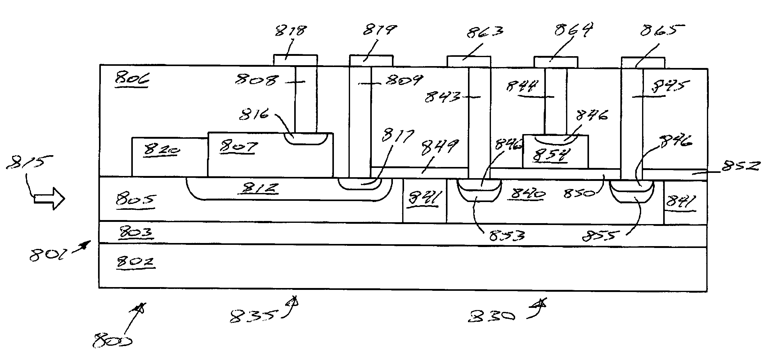
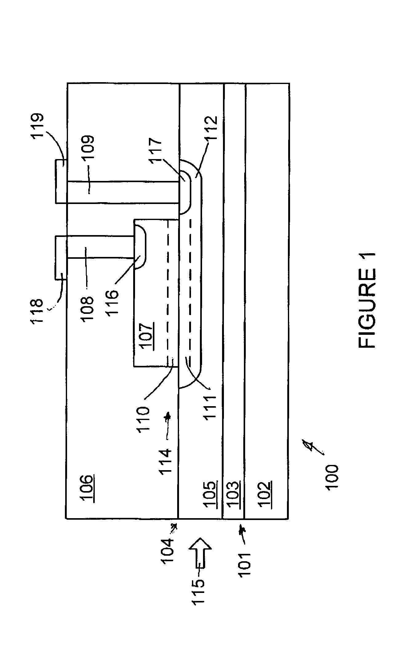
[0018]FIG. 1 is a side view of a waveguide photodetector 100, not to scale, according to a preferred embodiment of the present invention. The substrate 101 is made of silicon dioxide layer 103 on top of silicon layer 102. A silicon planar waveguide 104 receives an optical signal 115 from a source, not shown, to the left of the photodetector.

[0019]The waveguide 104 is made of a silicon core 105 and surrounded by cladding in the form of one or more dielectric layers. The cladding includes the silicon dioxide layer 103 underneath the silicon core and the dielectric films 106. On top of the waveguide core 105, is a layer of germanium 107. A germanium on silicon heterojunction is formed by the germanium layer 107 on top of the silicon core 105 of the waveguide 104. The waveguide core and heterojunction are surrounded on their sides and from above by one or more dielectric cladding layers 106. The dielectric layers 106 can also be referred to as inter-layer dielectric films. Some of the d...


PUM


Abstract

A germanium on silicon waveguide photodetector disposed on a silicon on insulator (SOI) substrate. The photodetector is incorporated into a section of a planar silicon waveguide on the substrate. The photodetector generates an electric current as an infrared optical signal travels through the photodetector.

Description

CROSS-REFERENCE TO RELATED APPLICATIONS[0001]This application claims priority from U.S. Provisional applications No. 60 / 389,962 filed Jun. 19, 2002, No. 60 / 391,277 filed Jun. 24, 2002, No. 60 / 432,925 filed Dec. 12, 2002 and No. 60 / 433,470 filed Dec. 13, 2002.FIELD OF THE INVENTION[0002]The present invention relates to a semiconductor waveguide photodetector and its use in a monolithic integrated circuit for the conversion of optical signals to electrical signals.BACKGROUND OF THE INVENTION[0003]The rapid expansion in the use of the Internet has resulted in a demand for high speed communications links and devices, including optical links and devices. Optical links using fiber optics have many advantages compared to electrical links: large bandwidth, high noise immunity, reduced power dissipation and minimal crosstalk. Optoelectronic integrated circuits made of silicon are highly desirable since they could be fabricated in the same foundries used to make VLSI integrated circuits. Opti...

Claims


Application Information

Patent Timeline
IPC IPC(8): G02F1/35
CPCH01L31/0232H01L31/109
Inventor GUNN, III, LAWRENCE C.PINGUET, THIERRY J.RATTIER, MAXIME JEANCAPELLINI, GIOVANNI
Owner CISCO TECH INC
Why Eureka
Try Eureka