Packaging method for an electronic element

a technology of electronic elements and packaging methods, applied in the direction of individual semiconductor device testing, semiconductor/solid-state device testing/measurement, instruments, etc., can solve the problems of reducing the production rate of ic or led devices, complicated and laborious process of attaching solder balls (b>80/b>) to dies, and unpredictable effects on physical characteristics of ics, etc., to improve the production rate of integrated circuits and reduce the cost of ic and led devices

Inactive Publication Date: 2008-12-02
MUTUAL PAK TECH
View PDF7 Cites 31 Cited by
  • Summary
  • Abstract
  • Description
  • Claims
  • Application Information

AI Technical Summary

Benefits of technology

[0020]The main objective of the invention is to provide a packaging method for an IC or an LED that can be widely used, improves the production rate of an integrated circuit (IC) or light emitting diode (LED) device and lowers the cost of the IC and LED devices.

Problems solved by technology

However, bonding wires (71, 71a) from the IC die (70) and the LED die (70a) respectively to the pins (61, 61a) have unpredictable affects on the physical characteristics of the IC and LED devices such as heat conduction, inductance and impedance.
Furthermore, positioning and attaching the wires (71, 71a) significantly reduces the production rate of the IC or LED devices.
The process of attaching the solder balls (80) to the die (80) is complicated and tedious and takes time.
2. The die is made of a segment of a silicon wafer, GaAs or Sapphire that is fragile and the metal bonding pad is very poor on adhesion.
Attaching solder balls (80) directly to the die (80) with a poor adhesion bonding pads has a high probability of damaging or destroying the die (80) during the packaging process.

Method used


Image

  • Packaging method for an electronic element
  • Packaging method for an electronic element
  • Packaging method for an electronic element

Examples


Embodiment Construction

[0036]With reference to FIGS. 8, a packaging method for an integrated circuit (IC) and light emitting diode (LED) comprises:

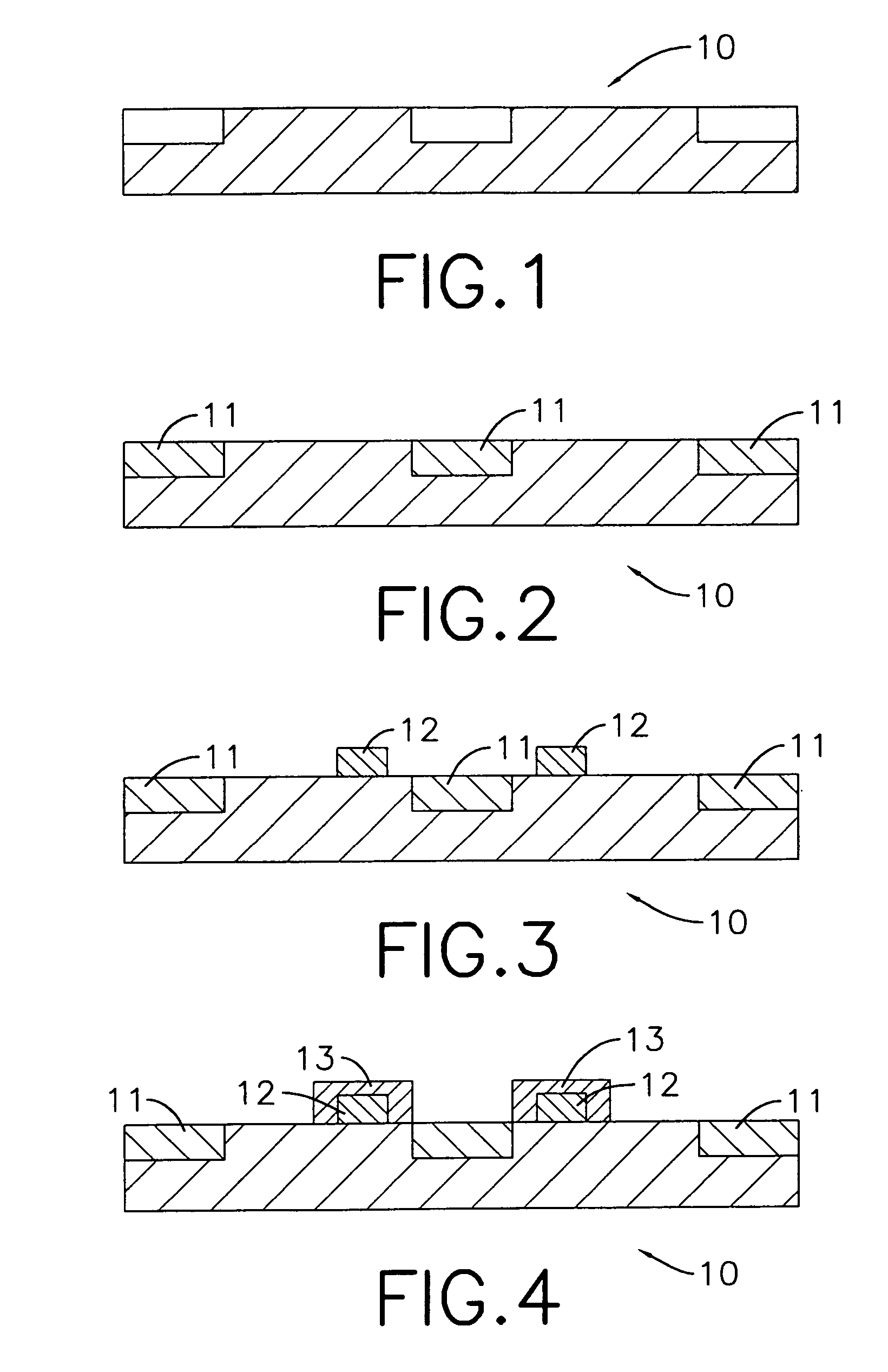
[0037](A) etching portions of a top surface of a metal board (10) made of copper to form several recesses between raised unetched segments (FIG. 1) and filling the recesses with a dielectric material (11) of high metal density polymer (FIG. 2);

[0038](B) forming multiple metal or solder balls (12) on the raised unetched segments by plating or printing (FIG. 3);

[0039](C) coating the solder balls (12) with a thin metal paste layer (13) made of silver (Ag) or tin (Sn) flux (FIG. 4);

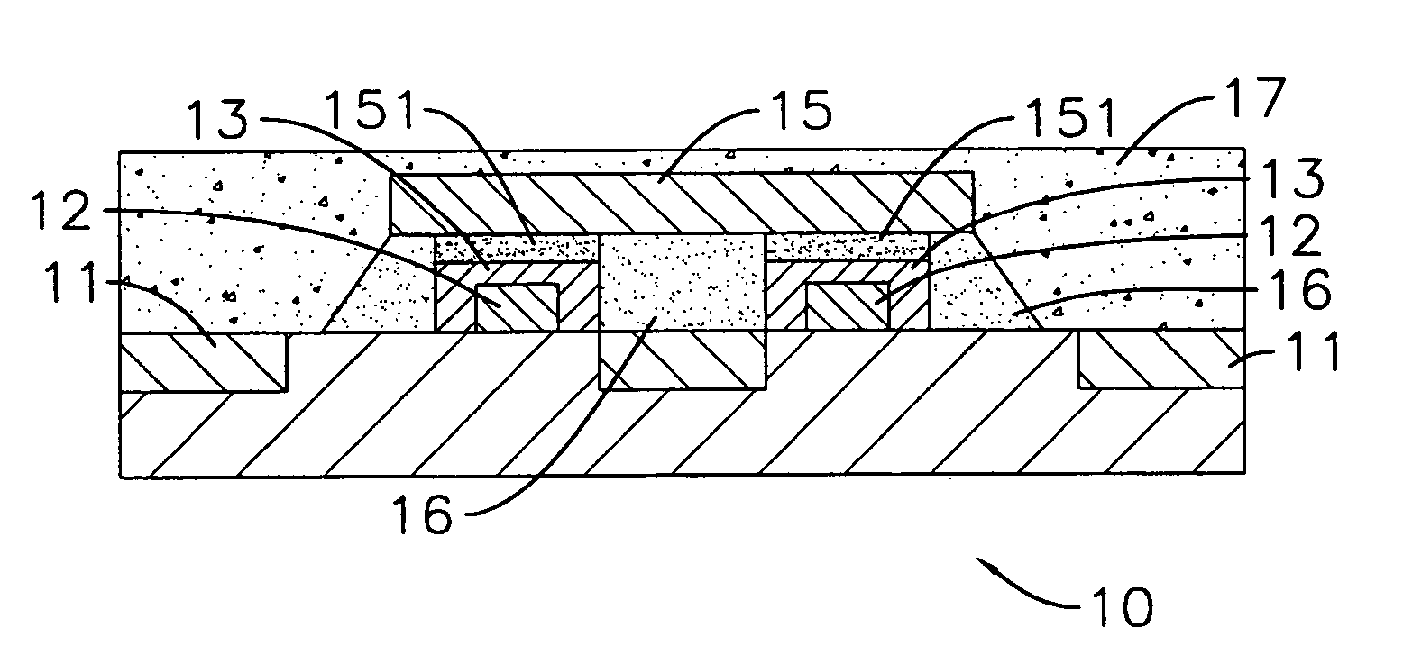
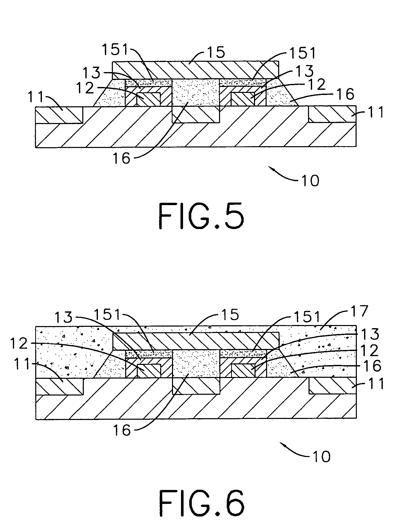
[0040](D) bonding contacts (151) on an IC or LED die (15) respectively to the solder balls (12) with the thin metal paste layer (13) (FIG. 5);

[0041](E) injecting an underfill (16) between the die (15) and the metal board (10) (FIG. 5);

[0042](F) sealing the die (15) with an outer encapsulant (17) (FIG. 6); when the die (15)is an LED, the outer encapsulant (17) is transparent to allow ligh...


PUM

PropertyMeasurementUnit
densityaaaaaaaaaa
transparentaaaaaaaaaa
heat conductionaaaaaaaaaa

Abstract

A packaging method for an electronic element has: etching portions of a top surface of a metal board to form recesses between raised unetched segments and filling the recesses with a dielectric material of high density polymer; forming multiple solder balls respectively on the raised unetched segments; coating the solder balls with a thin flux layer; bonding contacts on a die respectively to the solder balls with the thin flux layer; injecting an encapsulant between the die and the metal board; sealing the die with an outer encapsulant; etching a bottom surface of the metal board to form multiple metal leads; coating the bottom surface of the metal board other than the metal leads with a solder resist; and conducting a continuity test. The solder balls are not formed directly on the fragile die so the packaging method can be used with any types of dies and has a good applicability.

Description

BACKGROUND OF THE INVENTION[0001]1. Field of the Invention[0002]The present invention relates to a packaging method for an electronic element, and more particularly to a packaging method for an IC or an LED and that lowers the cost of the IC or LED package.[0003]2. Description of Related Art[0004]Semiconductors are used with virtually all electronic equipment including personal computers, cell phones and automated teller machines (ATM). These pieces of equipment all have printed circuit boards (PCB) with IC chips and other electronic elements derived from semiconductor technologies. One of the semiconductor technologies is a packaging technology.[0005]With reference to FIGS. 9 and 10, a conventional packaging method for an integrated circuit (IC) or a light emitting diode (LED) in accordance with the prior art comprises:[0006]bonding an IC die (70) or an LED die (70a) respectively to a lead frame (60) or a copper clad laminate (60a);[0007]bonding multiple wires (71, 71a) respectivel...

Claims


Application Information

Patent Timeline
Patent Type & Authority Patents(United States)
IPC IPC(8): H01L21/00
CPCH01L21/4832H01L23/3135H01L23/49582H01L24/16H01L24/28H01L24/81H01L21/563H01L2224/32225H01L33/486H01L33/62H01L2221/68377H01L2224/13099H01L2224/16225H01L2224/48247H01L2224/73203H01L2224/81192H01L2224/81801H01L2224/83102H01L2224/92125H01L2924/01005H01L2924/01029H01L2924/01047H01L2924/0105H01L2924/01078H01L2924/01079H01L2924/01082H01L2924/10329H01L2924/14H01L2924/15311H01L2924/30107H01L2924/3011H01L24/48H01L2924/00014H01L2924/01006H01L2924/014H01L2224/16227H01L2924/0132H01L2224/2919H01L2924/157H01L2224/29111H01L2924/12041H01L2224/13111H01L2224/16245H01L2224/73204H01L2924/10253H01L2224/45099H01L2924/01028H01L2924/00015H01L2924/00H01L24/05H01L2224/05001H01L2224/05023H01L2224/05568H01L2224/05611H01L2224/05639H01L2924/181H01L2224/05099H01L2924/00012
Inventor HWAN, LU-CHEN
Owner MUTUAL PAK TECH
Why Eureka
Try Eureka