

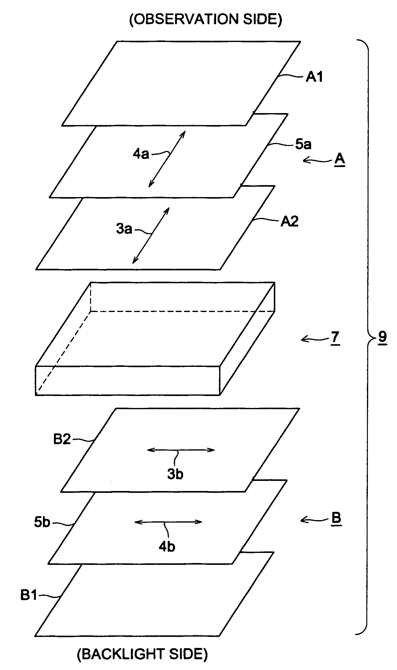
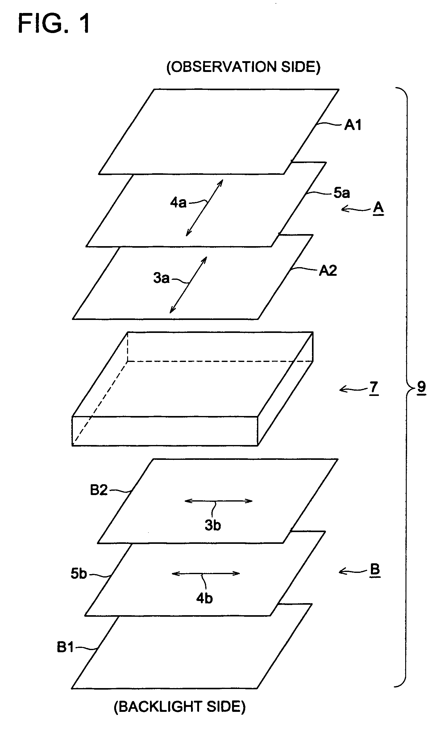
Liquid crystal display device
a liquid crystal display and display device technology, applied in the direction of instruments, polarising elements, thin material processing, etc., can solve the problems of large number of laminated films, high cost, defective products generated, etc., and achieve the effect of low cost, low color change, and low contras
- Summary
- Abstract
- Description
- Claims
- Application Information
AI Technical Summary
Benefits of technology
Problems solved by technology
Method used
Image

Examples
example
[0409]This invention will be described more specifically using the following working examples, but this invention is not to be limited by these examples.
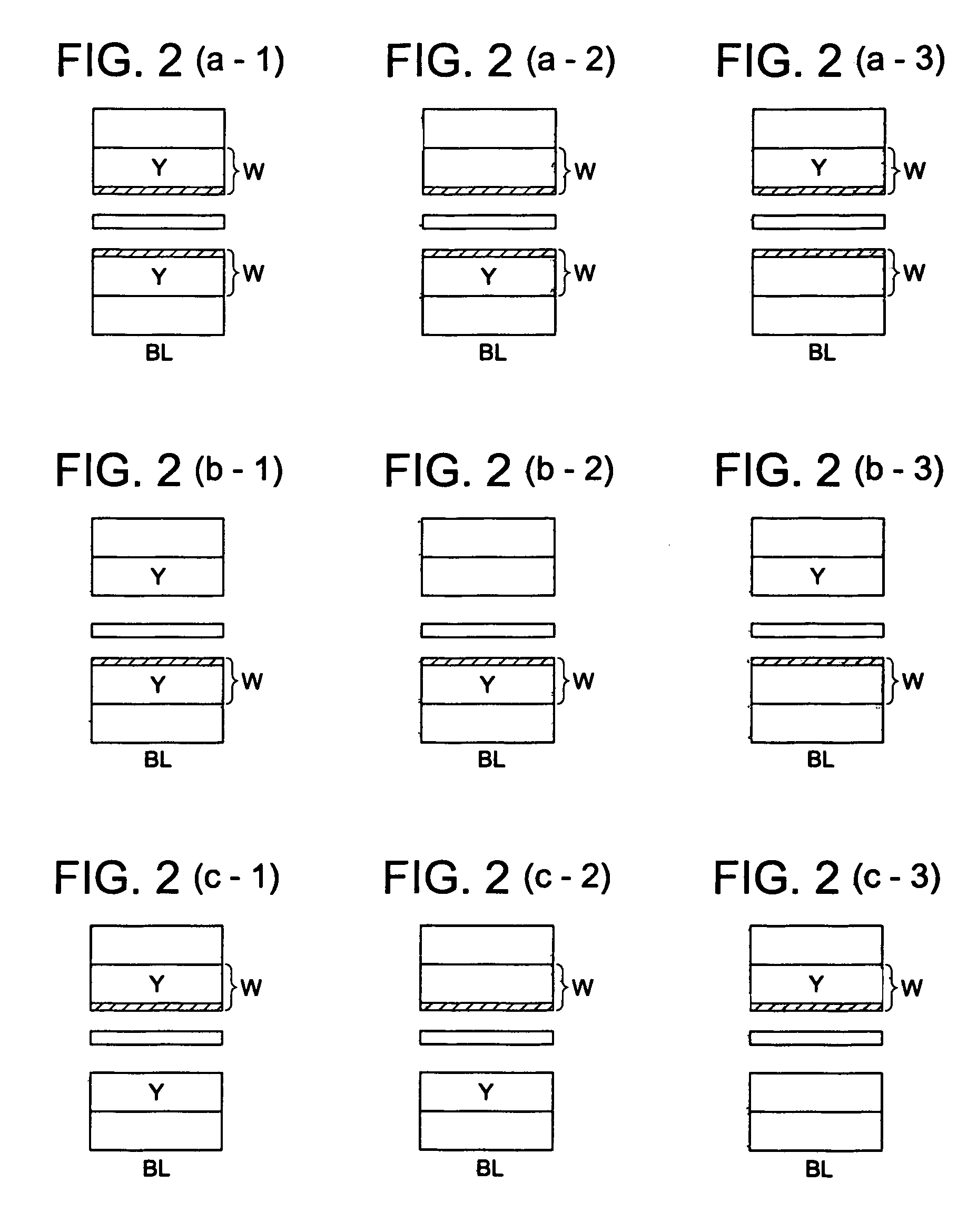
[0410](Preparation of the Cellulose Ester Film A)
[0411](Silicon Dioxide Dispersing Solution A)
[0412]
Aerosil 972 V (Manufactured by Japan Aerosil)12 parts by weight(average diameter of primary particles 16 nm,apparent density 90 g / liter)Ethanol88 parts by weight
[0413]The substances listed above were agitated and mixed in a dissolver for 30 minutes and then dispersion was performed using Manton Gaulin. 88 parts by weight of methylene chloride were loaded to the silicon dioxide dispersing solution while stirring and the resultant was agitated and mixed for 30 minutes using a dissolver to thereby prepare the silicon dioxide dispersing solution diluent A.
[0414](Preparation of In-line Additive A)
[0415]
TINUVIN 109 (Manufactured by Chiba Specialty11 parts by weightChemicals)TINUVIN 171 (Manufactured by Chiba Specialty 5 parts by weightChemi...
PUM
| Property | Measurement | Unit |
|---|---|---|
| thickness direction retardation | aaaaa | aaaaa |
| thickness | aaaaa | aaaaa |
| mass % | aaaaa | aaaaa |
Abstract
Description
Claims
Application Information