Double data rate system

a double data rate and memory technology, applied in the field of memory interface circuitry, can solve the problems of difficult design of phy circuitry for interfacing with double data rate (ddr) memories, adverse effects on clock and signal timing, and adverse effects on clock generation or reproduction circuitry

Active Publication Date: 2008-12-30
QUALCOMM INC
View PDF11 Cites 16 Cited by
  • Summary
  • Abstract
  • Description
  • Claims
  • Application Information

AI Technical Summary

Benefits of technology

[0007]These and other aspects of the invention are more fully comprehended on review of this disclosure.

Problems solved by technology

Design of PHY circuitry for interfacing with double data rate (DDR) memories, for example, may be difficult.
Furthermore, clock and signal timing may be adversely affected by a number of factors.
Clock generation or reproduction circuitry may also be adversely impacted by power supply voltage variations and power supply related noise, particularly when used with circuitry using high switching frequencies.
Clock and timing may also be unduly affected by provision of multiple power supply domains, which may be required for analog circuits and digital circuits, by voltage gradients within or across power supply domains, particularly larger size domains, and at transitions across power supply domains.
Moreover, resolution of timing related issues, whether it is distortion of a data eye or clock skew, may be difficult.
Ensuring that a circuit design meets appropriate timing budgets may often be a time consuming process, often requiring the use of skilled personnel and complicated analysis for every design.
Further, often when a circuit design does meet the appropriate timing budget and other constraints, the design is only valid for the particular circuit, and the circuit cannot be extended for use with additional memories without re-design and concomitant time consuming time budget revivification.

Method used


Image

  • Double data rate system
  • Double data rate system
  • Double data rate system

Examples


Embodiment Construction

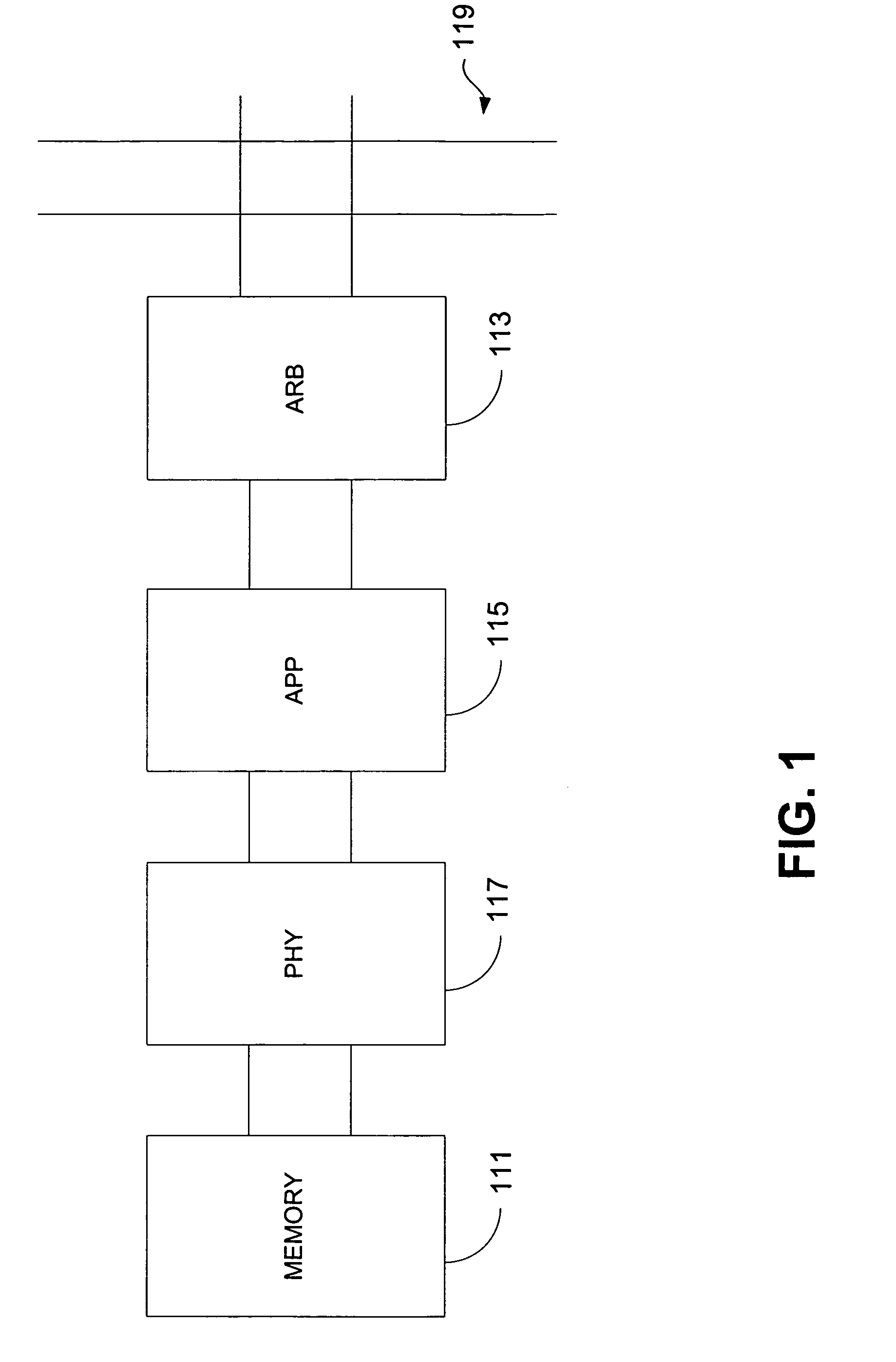
[0015]FIG. 1 is a block diagram of a memory 111 and memory controller. The memory retains information. A system accesses the memory, for reads and / or writes, by way of the memory controller. The memory controller is shown in FIG. 1 with a physical layer (PHY) 117, an application layer 115, and an arbitration layer 113. The arbitration layer generally includes port arbitration logic, data formatting logic for external bus formats, and logic for other functions. As illustrated, the arbitration layer is conceptually shown as connected to a bus 119. The application layer generates control information specific to the protocol used by the particular memory.

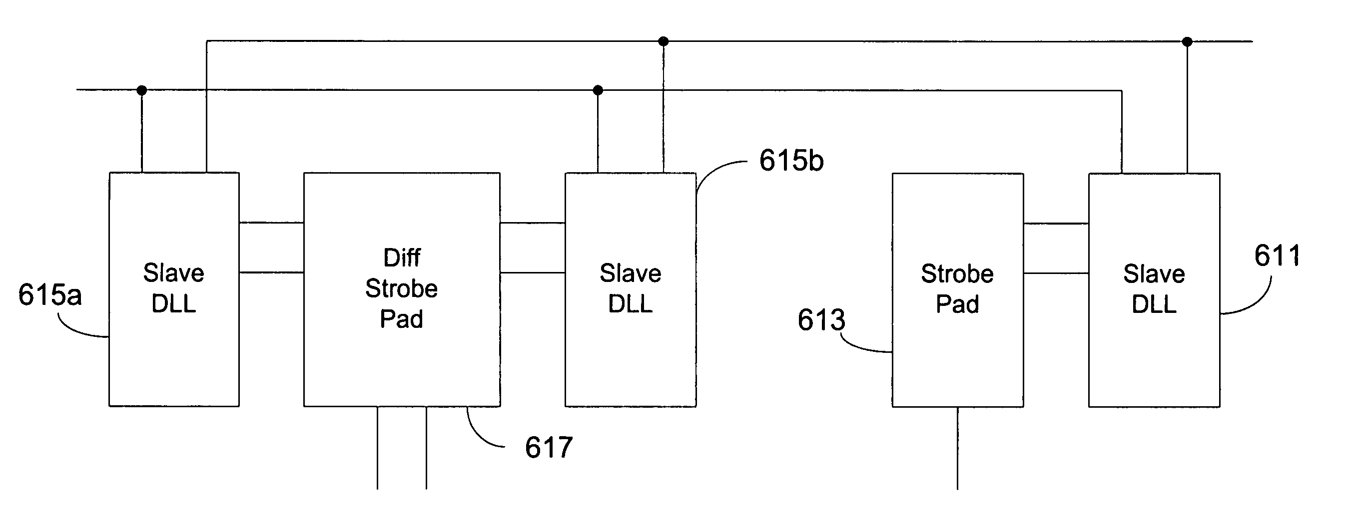
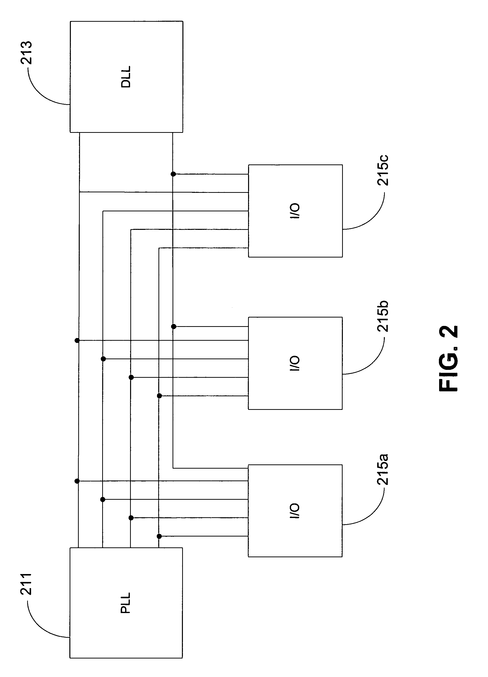
[0016]The PHY transmits signals to the memory and receives signals from the memory. The signals generally include data signals to be written to the memory, data signals read from the memory, a differential clock signal provided to the memory, and a bidirectional data strobe (DQS) signal. The DQS signal is provided by the PHY on data wri...


PUM


Abstract

An extendible timing architecture for an integrated circuit is disclosed. The extendible timing architecture provides metal programmable components for use with different operational clock frequencies. In some embodiments the architecture utilizes master / slave DLLs with a double data rate memory circuit.

Description

BACKGROUND[0001]The invention relates generally to memory interface circuitry, and more particularly to extendible timing circuitry for double data rate memory applications.[0002]Memory interface circuitry generally may include arbitration circuitry, application specific circuitry, and physical layer interface circuitry. This circuitry is generally provided by an asynchronous integrated circuit (ASIC) separate from the memory. The arbitration circuitry generally performs functions relating to accessing a system bus using an implementation specific bus protocol and otherwise formats transmitted and received data and instructions as appropriate. The application specific circuitry generally includes control circuitry for generating memory access commands and circuitry for generally controlling interaction with a memory. The physical (PHY) circuitry transmits signals from the ASIC to the memory and receives signals from the memory.[0003]Design of PHY circuitry for interfacing with doubl...

Claims


Application Information

Patent Timeline
Patent Type & Authority Patents(United States)
IPC IPC(8): G06F1/12G06F1/00H03L5/00
CPCG06F1/04
Inventor MALEKKHOSRAVI, BEHNAMSHAIKLI, NADIM HASHIM
Owner QUALCOMM INC
Why Eureka
Try Eureka