Optical microstructures for light extraction and control

a microstructure and optical technology, applied in the field of optical microstructures for light extraction and control, can solve the problems of inefficient light coupling, inability to reach the viewer, and inefficient material at all times, so as to improve contrast, enhance the light extraction process, and increase the probability of light wave release

Inactive Publication Date: 2009-02-03
RAMBUS DELAWARE
View PDF153 Cites 78 Cited by
  • Summary
  • Abstract
  • Description
  • Claims
  • Application Information

AI Technical Summary

Benefits of technology

[0010]The present invention enhances the light extraction process by introducing optical microstructures on one or both surfaces of the active layer. Since the active layer has both an input and an output function, means for enhancing both are envisioned. The input function to the active layer occurs on the internal surface, so this is where an embodiment of the present invention adds a collector-coupler, a means for facilitating migration of light from the waveguide into the active layer. An opaque material may be disposed interstitially between the collector-couplers to improve contrast. This opaque material can be electrically conductive which in turn can be used in actuating the pixel. The output function occurs on the external surface, so at this location an embodiment of the present invention adds a collimator, a means for both increasing the probability that a light wave will be released from the active layer, and improving the apparent intensity by redirecting light waves so that more of them reach the viewer. Issues such as stiction and pixel-to-pixel crosstalk are mitigated through advantageous selection of materials and geometries.

Problems solved by technology

Where the pixel does not exist (e.g., inactive regions between pixels), very inefficient light coupling is desired.
In the locations between all of the pixels, the material is inefficient at FTIR at all times.
These modes result in some light not reaching the viewer.
Previous embodiments have exhibited imperfect results in turning off the pixel controllably within such a time frame.

Method used


Image

  • Optical microstructures for light extraction and control
  • Optical microstructures for light extraction and control
  • Optical microstructures for light extraction and control

Examples


Embodiment Construction

[0029]In the following description, numerous specific details are set forth to provide a thorough understanding of the present invention. However, it will be apparent to those skilled in the art that the present invention may be practiced without such specific details. In other instances, detailed physical features are idealized in order not to obscure the present invention in unnecessary detail. For the most part, details considering timing considerations and the like have been omitted inasmuch as such details are not necessary to obtain a complete understanding of the present invention and are within the skills of persons of ordinary skill in the relevant art.

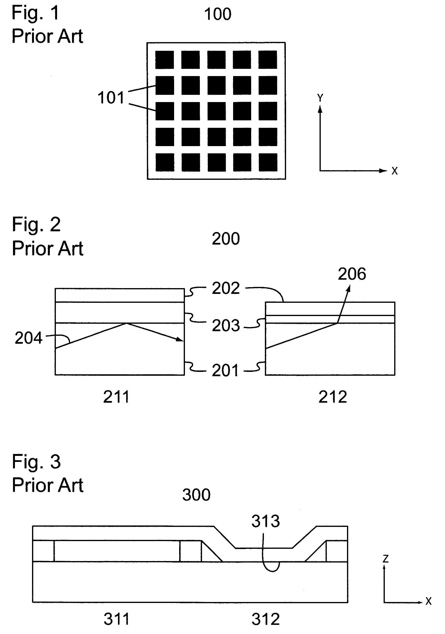
[0030]The general concept of TMOS, as originally expressed in U.S. Pat. No. 5,319,491, is briefly illustrated in FIGS. 2 and 3. In FIG. 2, a side view 200 of one pixel 101 is shown, first in the “off” position 211, and second in the “on” position 212. An internal light guide 201, and the light waves 204 contained therein, are...


PUM


Abstract

The application of microstructures which improve the quality of light available to the viewer of an optical display system, or any display which works on the concept of moving one surface into direct contact or close proximity of a light guide to extract light through frustrated total internal reflection. Optical microstructures are introduced on one or both of the surfaces of the active layer to enhance its performance. Since the active layer has both an input and an output function, means for enhancing both are presented. The input function to the active layer occurs on the internal surface, so this is where the present invention adds a collector-coupler, a means for facilitating the migration of light from the waveguide into the active layer. The output function occurs on the external surface, where the present invention adds a collimator, a means for both increasing the probability that a light wave will be released from the active layer, and improving the apparent intensity by redirecting light waves so that more of them reach the viewer. Compound microlenses on the internal surface of the active layer can serve as both collector-couplers and collimators, substantially improving light extraction from the light guide and light distribution to the viewer. Depositing a reflective or colored material in the interstitial spaces between these compound microlenses improves the contrast ratio and mitigate pixel cross-talk. The opaque material can be conductive for use in actuating the display.

Description

TECHNICAL FIELD[0001]The present invention primarily relates to the field of displays, and more generally to any display system in which light is extracted from a waveguide through means of selectively controllable contact with its surface.BACKGROUND INFORMATION[0002]The present invention addresses certain embodiments for improvement that occur when creating an optical display system, or any device which works on the concept of frustrated total internal reflection (FTIR), an example of which is the Time Multiplexed Optical Shutter (TMOS) display disclosed in U.S. Pat. No. 5,319,491, which is hereby incorporated by reference herein. Embodiments for improvement arise with respect to three basic optical materials in the design of a FTIR display. In a display application, there are defined locations within the architecture where a pixel nominally exists. Where this pixel exists, efficient light coupling from a light guide is desired when FTIR occurs (by controllable switching of the pix...

Claims


Application Information

Patent Timeline
Patent Type & Authority Patents(United States)
IPC IPC(8): G02B6/26
CPCG02B6/00G02B6/122G02B6/125G02B6/2852G09G3/3473G02B6/351G02B6/12
Inventor VAN OSTRAND, DANKING, CAREYGOBELL, GARTH
Owner RAMBUS DELAWARE
Why Eureka
Try Eureka