Method for using a multiple polarity reversible charge pump circuit

a charge pump and multiple polarity technology, applied in the field of capacitor voltage multiplier circuits, can solve the problems of increasing the current that must be supplied by the user, requiring significant amount of semiconductor real estate for their implementation, and requiring significant amount of power supply by the user, and achieves large current and high leakage current.

Active Publication Date: 2009-02-24
SANDISK TECH LLC
View PDF53 Cites 35 Cited by
  • Summary
  • Abstract
  • Description
  • Claims
  • Application Information

AI Technical Summary

Benefits of technology

[0016]While the present invention is useful in numerous circuits incorporating any of a wide variety of devices and structures, the invention is particularly beneficial when used with certain erasable memory array technologies, such as those incorporating certain resistive passive element memory cells. Such cells tend to have high leakage current when programming and erasing, and a memory array, particularly a three-dimensional memory array, therefore requires large currents at the required programming and erasing voltages. For example, in a program operation, the positive voltage charge pump may need to deliver a particularly high value of output current, while in an erase operation the negative voltage charge pump may need to deliver a particularly high value of output current (e.g., greater than any current needed at a boosted positive voltage).
[0017]Such large output currents require large charge pumps. However, it is undesirable to build two very large charge pumps if one of them (e.g., a negative voltage charge pump) is only utilized for certain mode(s) of operation. A multiple polarity reversible charge pump circuit, as described herein, allows a much smaller, lower power charge pump circuit to generate the required voltages at the required output currents.
[0018]The invention in several aspects is particularly suitable for implementation within an integrated circuit, including those integrated circuits having a memory array, for methods for operating such circuits, for systems incorporating such circuits, and for computer readable media encodings of such circuits, all as described herein in greater detail and as set forth in the appended claims. A wide variety of such integrated circuits is specifically contemplated, including those having a three-dimensional memory array formed above a substrate.
[0019]The foregoing is a summary and thus contains, by necessity, simplifications, generalizations and omissions of detail. Consequently, those skilled in the art will appreciate that the foregoing summary is illustrative only and that it is not intended to be in any way limiting of the invention. Other aspects, inventive features, and advantages of the present invention, as defined solely by the claims, may be apparent from the detailed description set forth below.

Problems solved by technology

Moreover, such voltage generator circuits also may consume a significant amount of power relative to the remainder of the circuit, and thus increase the current that must be supplied by the user (e.g., by the VDD power supply).
In addition, such voltage generator circuits also may also require a significant amount of semiconductor real estate for their implementation, particularly if a high output current or large magnitude voltage is required.
If the output current requirements for each voltage were both significant, each of these two charge pump circuits would require large pumping capacitors, and thus would consume considerable precious silicon area.
Such cells tend to have high leakage current when programming and erasing, and a memory array, particularly a three-dimensional memory array, therefore requires large currents at the required programming and erasing voltages.
Such large output currents require large charge pumps.
However, it is undesirable to build two very large charge pumps if one of them (e.g., a negative voltage charge pump) is only utilized for certain mode(s) of operation.

Method used


Image

  • Method for using a multiple polarity reversible charge pump circuit
  • Method for using a multiple polarity reversible charge pump circuit
  • Method for using a multiple polarity reversible charge pump circuit

Examples


Embodiment Construction

)

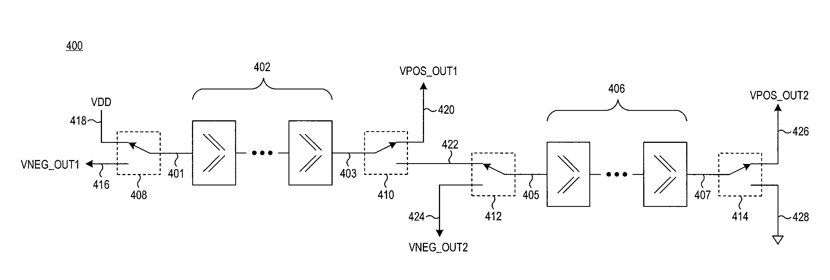
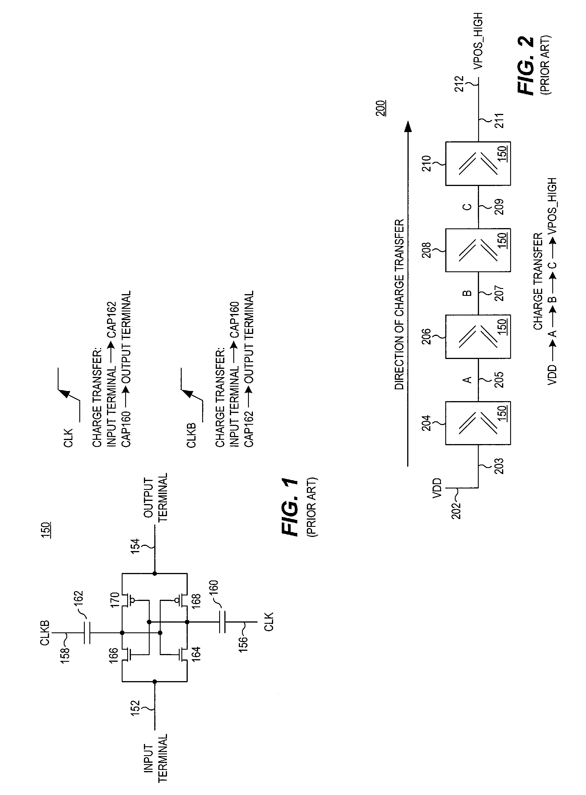
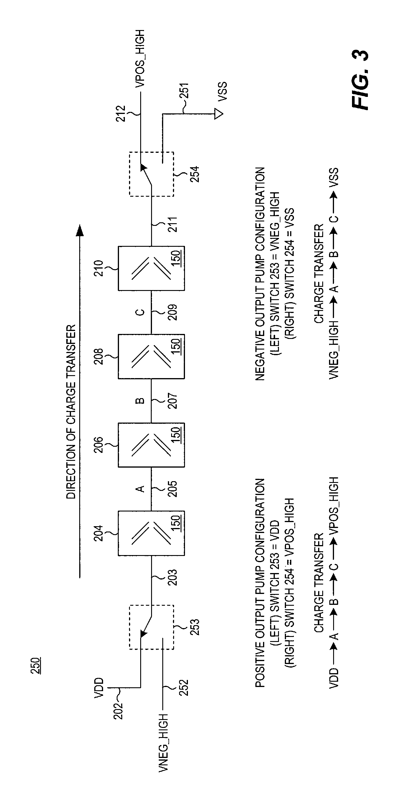
[0033]Referring now to FIG. 1, an exemplary directional charge pump stage 150 is depicted. Such a charge pump stage 150 is frequently incorporated as one of a plurality of series-coupled charge pump stages within a charge pump circuit.

[0034]The charge pump stage 150 is clocked by two complementary clocks CLK (also labeled 156) and CLKB (also labeled 158), and charge is always transferred from the input terminal 152 to the output terminal 154 (i.e., here shown as left to right). On a rising edge of the CLK signal, and during the time that CLK remains high, charge transfers from the input terminal 152 (i.e., “input node”), through NMOS transistor 166, to capacitor 162. During the same rising edge of the CLK signal, charge also transfers from capacitor 160, through PMOS transistor 168, to the output terminal 154.

[0035]On a rising edge of the CLKB signal, and during the time that CLKB remains high, charge transfers from the input terminal 152, through NMOS transistor 164, to capacitor ...


PUM


Abstract

A multiple polarity reversible charge pump circuit is disclosed which, in certain embodiments, may be configured to generate a positive voltage at times and may be reversed to generate a negative voltage at other times. Such a charge pump circuit is advantageous if both the positive and negative voltage are not simultaneously required. In certain other embodiments, a charge pump circuit generates a high output current for only a positive boosted voltage in one mode of operation, but lower current positive and negative boosted voltage outputs in another mode of operation. Use with certain erasable memory array technologies is disclosed, particularly certain resistive passive element memory cells, and more particularly in a three-dimensional memory array.

Description

CROSS-REFERENCE TO RELATED APPLICATION(S)[0001]This application is related to the following U.S. Application(s), each of which is incorporated by reference herein in it entirety:[0002]U.S. application Ser. No. 11 / 618,841 entitled “Multiple Polarity Reversible Charge Pump Circuit” by Ali K. Al-Shamma and Roy E. Scheuerlein, filed on even date herewith.BACKGROUND[0003]1. Field of the Invention[0004]The present invention relates to semiconductor voltage generator circuits, and particularly to capacitive voltage multiplier circuits.[0005]2. Description of the Related Art[0006]Many integrated circuits, particularly those using a single power supply voltage, incorporate on-chip circuitry to generate a “boosted” voltage having a magnitude greater than the power supply voltage. Frequently this boosted voltage is used as a veritable power supply voltage for portions of the circuitry contained on the integrated circuit. For example, certain types of semiconductor memories, such as “flash” EEP...

Claims


Application Information

Patent Timeline
Patent Type & Authority Patents(United States)
IPC IPC(8): G05F1/10
CPCH02M3/073H02M2003/071H02M2003/077H02M3/071H02M3/077
Inventor AL-SHAMMA, ALI K.SCHEUERLEIN, ROY E.
Owner SANDISK TECH LLC
Why Eureka
Try Eureka