Liquid crystal display device and manufacturing method thereof

a technology of liquid crystal display device and manufacturing method, which is applied in the direction of semiconductor devices, instruments, optics, etc., can solve problems such as complex processes, and achieve the effect of simplifying the manufacturing steps and improving the utilization efficiency of materials

Inactive Publication Date: 2009-03-03
SEMICON ENERGY LAB CO LTD
View PDF33 Cites 16 Cited by
  • Summary
  • Abstract
  • Description
  • Claims
  • Application Information

AI Technical Summary

Benefits of technology

[0007]In view of the aforementioned problem, according to the invention, the number of steps for forming a thin film transistor is reduced in order to reduce the production cost and improve the yield of an active matrix liquid crystal display device.
[0019]According to the invention, as a wiring layer and a mask can be directly patterned by ejecting composition, utilization efficiency of material can be improved. Moreover, manufacturing steps of a liquid crystal display device can be simplified.

Problems solved by technology

By using one photo mask in the manufacturing steps of a liquid crystal display device, steps such as resist coating, prebaking, exposure, development, and postbaking, as well as the formation of a covering film, etching, resist peeling, rinsing, drying and the like before and after the aforementioned steps are required, which make the process complicated.

Method used


Image

  • Liquid crystal display device and manufacturing method thereof
  • Liquid crystal display device and manufacturing method thereof
  • Liquid crystal display device and manufacturing method thereof

Examples


embodiment mode 1

[0060]A manufacturing method of a channel-etch type thin film transistor is described as Embodiment Mode 1.

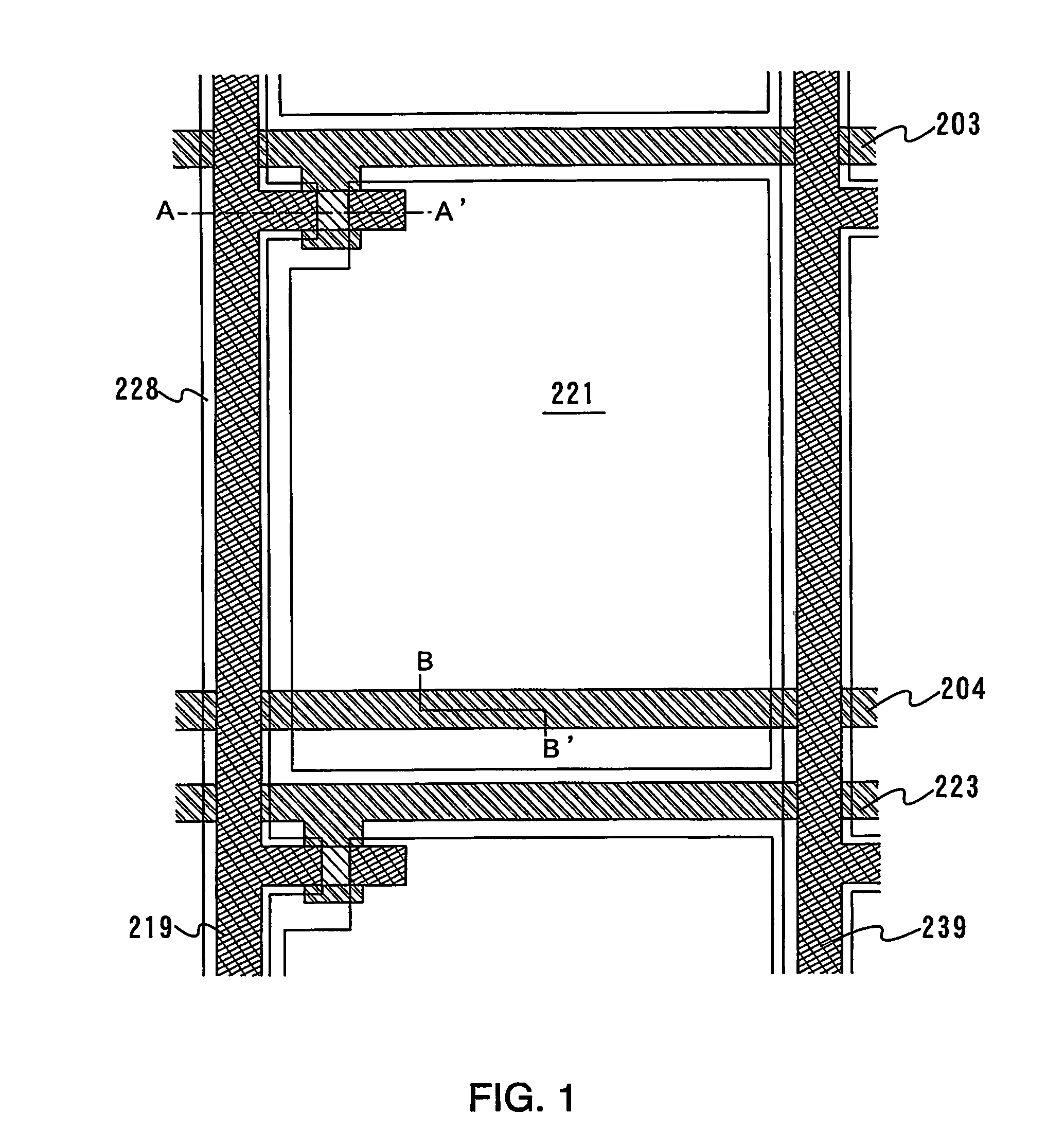
[0061]In this embodiment mode, a manufacturing method of a liquid crystal display device is described. A method for forming an inverted staggered TFT in a pixel portion on a substrate and a method for forming a storage capacitor connected to the TFT are described in details along the process. At the same time, a method for forming an input terminal portion provided in an end portion of the substrate for electrically connecting to a wiring of a circuit provided on another substrate is described.

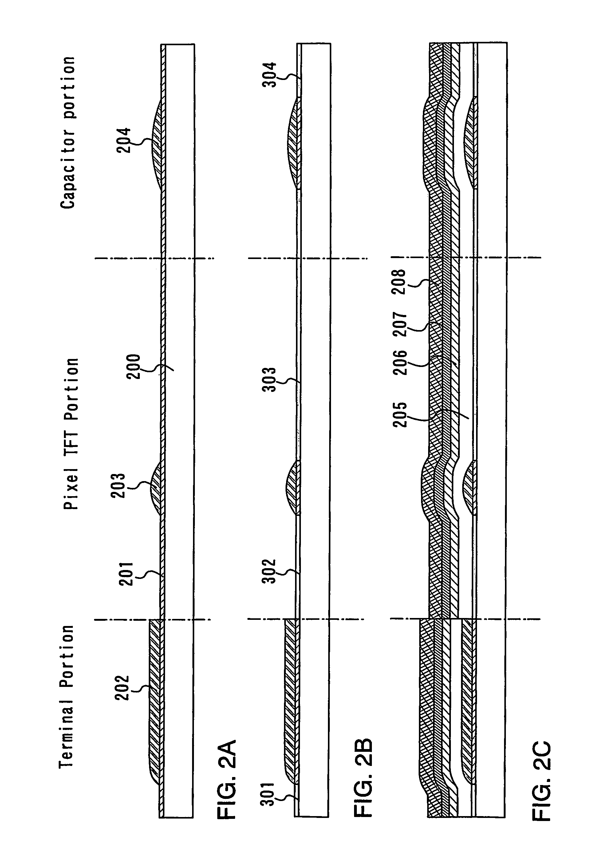
[0062]In FIG. 2A, a substrate 200 may be a non-alkali glass substrate such as a barium borosilicate glass, an aluminoborosilicate glass, or an aluminosilicate glass fabricated by fusion method and a float method, a ceramic substrate as well as a plastic substrate which can resist the processing temperature of the present manufacturing steps, and the like. Further, a semiconductor substrat...

embodiment mode 2

[0101]In this embodiment mode, a different mode than the aforementioned embodiment mode is described with reference to FIGS. 5A to 5C and 6A and 6B. In Embodiment Mode 1, the semiconductor film 206, the semiconductor film 207 and the metal film 208 are simultaneously etched as shown in FIG. 3A, however, the insulating film 205 may be etched at the same time as well. FIGS. 5A to 5C show steps in this case. Note that steps up to the formation of the metal film 208 may be similar to Embodiment Mode 1, therefore, description thereof is omitted here.

[0102]After the up to FIG. 5A, masks 209 and 309 are formed by selectively ejecting composition on the conductive film 208. Next, a wiring and an electrode are formed by removing an unnecessary portions by etching with the masks 209 and 309 (FIG. 5B), for which wet etching or dry etching is employed. At this time, the insulating film 205, the semiconductor film 206, the semiconductor film 207 and the metal film 208 are etched while an insulat...

embodiment mode 3

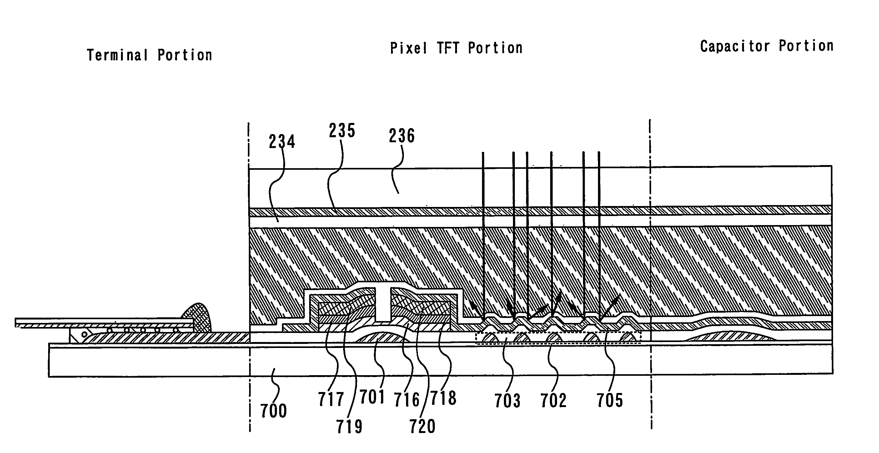
[0107]In this embodiment mode, a different mode than the aforementioned embodiment modes is described with reference to FIG. 7. Note that the same portions as those in the aforementioned embodiment modes are denoted by the same reference numerals in FIG. 7.

[0108]First, an insulating film as a protective film is formed after obtaining a state of FIG. 4A according to Embodiment Mode 1. The insulating film is formed by selectively ejecting composition. An insulating film 240 and an insulating film 241 are formed in a pixel TFT portion and a terminal portion respectively. Note that the insulating films 240 and 241 function as passivation films.

[0109]Moreover, an inorganic insulating film such as a silicon oxide film, a silicon nitride film, a silicon oxynitride film, and a tantalum oxide film may be formed in a single layer or a laminated structure. In this case, since a thin inorganic insulating film is formed on the entire surface, the insulating films 240 and 241 are formed by formin...


PUM

PropertyMeasurementUnit
thicknessaaaaaaaaaa
temperatureaaaaaaaaaa
pressureaaaaaaaaaa

Abstract

By using one photo mask in the manufacturing steps of a liquid crystal display device, steps such as resist coating, prebaking, exposure, development, and postbaking, as well as the formation of a covering film, etching, resist peeling, rinsing, drying and the like before and after the aforementioned steps are required, which make the process complicated. To solve the problem, a channel-etch type bottom gate TFT (inverted staggered TFT) is employed to pattern source and drain regions and a pixel electrode with the same mask. Moreover, according to the invention, among the patterns required to form a liquid crystal display device such as a conductive layer for a wiring layer or an electrode, a mask for forming a predetermined pattern and the like, at least one or more of them is formed by a method by which a pattern can selectively be formed, thereby manufacturing a liquid crystal display device.

Description

TECHNICAL FIELD[0001]The present invention relates to a liquid crystal display device having a circuit formed of a thin film transistor (TFT) and to a manufacturing method thereof.BACKGROUND ART[0002]In recent years, a technology to form a thin film transistor by using a semiconductor thin film (film thickness of about several nm to several hundred nm) formed on a substrate having an insulating surface is attracting attentions. A thin film transistor, which is widely applied to electronic devices such as an IC and an electronic optical device, is rapidly developed in particular as a switching element of an image display device.[0003]In general, a liquid crystal display device is known as an image display device using a thin film transistor. An active matrix liquid crystal display device is becoming to be more used which can provide an image in higher resolution as compared to a passive matrix liquid crystal display device. In an active matrix liquid crystal display device, a pixel e...

Claims


Application Information

Patent Timeline
Patent Type & Authority Patents(United States)
IPC IPC(8): G02F1/136G02F1/1368H01L21/288
CPCG02F1/1368H01L2224/16225H01L2224/32225H01L2224/48091H01L2224/48227H01L2224/48464H01L2224/73204H01L2224/73265H01L2924/181H01L2924/00014H01L2924/00012H01L2924/00G02F1/136
Inventor MAEKAWA, SHINJIYAMAZAKI, SHUNPEIKUWABARA, HIDEAKIMORIYA, YOSHITAKA
Owner SEMICON ENERGY LAB CO LTD
Why Eureka
Try Eureka