Optical receiver preamplifier

a receiver and optical technology, applied in the direction of amplifier modifications to reduce non-linear distortion, gain control, electromagnetic transceivers, etc., can solve the problems of low output voltage, waveform distortion, and small transmission loss in the fiber, so as to reduce the current-voltage conversion element and suppress the saturation of the output voltage. , the effect of current flowing

Active Publication Date: 2009-03-10
PANASONIC SEMICON SOLUTIONS CO LTD
View PDF10 Cites 2 Cited by
  • Summary
  • Abstract
  • Description
  • Claims
  • Application Information

AI Technical Summary

Benefits of technology

[0035]According to the present invention, by flowing part of an input current in a third transistor, a current flowing in a current-voltage conversion element can be reduced. Thus, saturation of an output voltage can be suppressed, and an input dynamic range can be expanded. Unlike a known structure, a value of a feedback resistor is not directly modulated by a transistor connected in parallel to the current-voltage conversion element, but by the operation of the third transistor, an excessive input current is bypassed and an open gain of the inverting amplifier is reduced. Thus, the operation of an inventive optical receiver preamplifier does not become unstable. Therefore, a stable operation and a wide input dynamic range characteristic, which have been in the trade-off relationship in the known technique, can be realized at the same time.

Problems solved by technology

In contrast, if a signal transmission distance through an optical fiber is short, a transmission loss in the fiber becomes small.
Therefore, when a current-voltage conversion gain (transimpedance gain) of the optical receiver preamplifier is increased to detect a small signal, at a time of inputting a large signal, an output voltage is saturated and a waveform is distorted and the signal can not be precisely detected.
On the other hand, when the current-voltage conversion gain is reduced to lower saturation of the output voltage, at a time of inputting a small signal, the small signal can not be sufficiently amplified and detection of a small signal is difficult.

Method used


Image

  • Optical receiver preamplifier
  • Optical receiver preamplifier
  • Optical receiver preamplifier

Examples


first embodiment

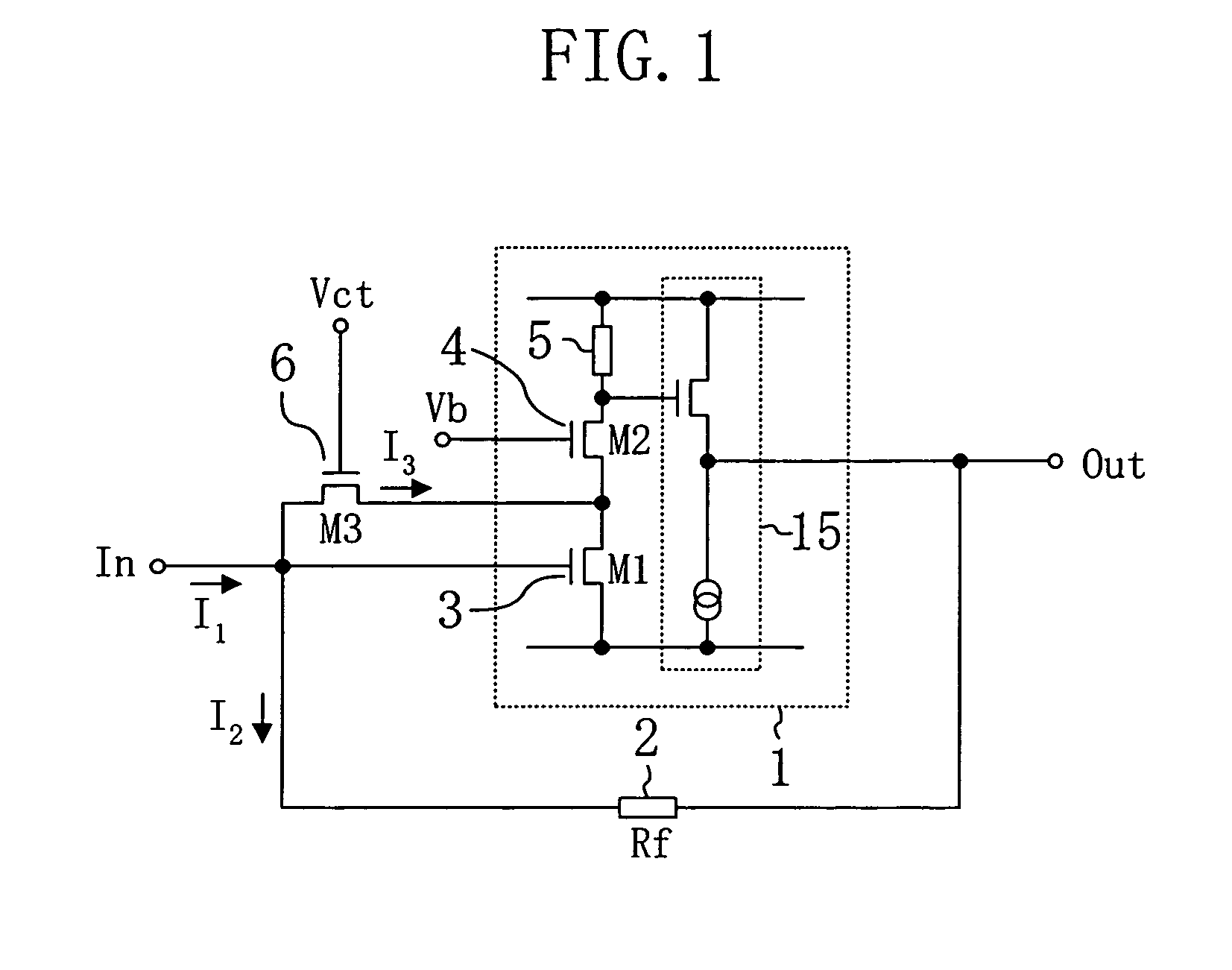
[0070]Hereinafter, an optical receiver preamplifier according to a first embodiment of the present invention will be described with reference to the accompanying drawings.

[0071]FIG. 1 illustrates a schematic configuration of the optical receiver preamplifier of the first embodiment.

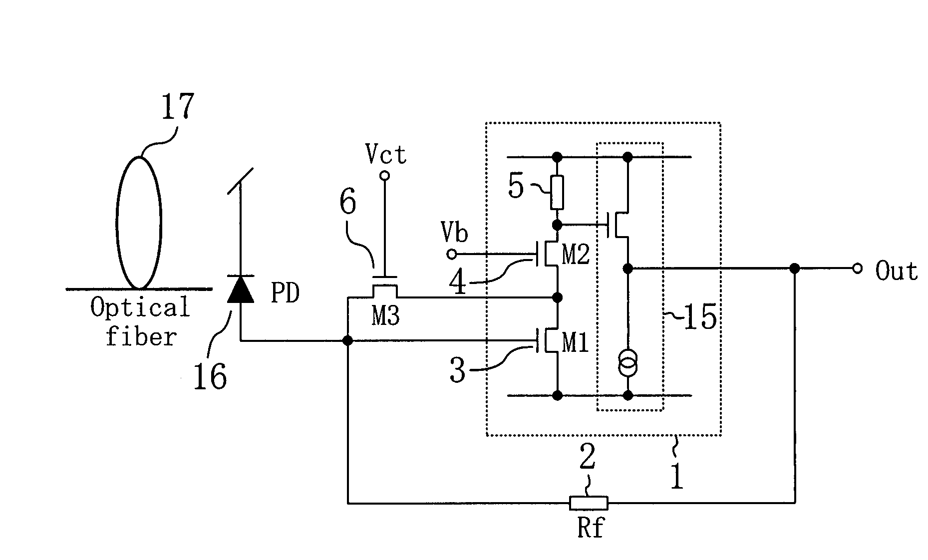
[0072]As shown in FIG. 1, the optical receiver preamplifier of the present invention is a transimpedance type preamplifier including an inverting amplifier 1 and a current-voltage conversion element (RF) 2 connected between an input terminal In and an output terminal Out of the inverting amplifier 1. In this embodiment, as the current-voltage conversion element 2, for example, a normal resistor is used.

[0073]A first feature of this embodiment is that the inverting amplifier 1 includes a first transistor (M1) 3 having a source connected to the ground and a gate connected to the input terminal In of the inverting amplifier 1, a second transistor (M2) 4 having a source connected to a drain of the first trans...

second embodiment

[0078]Hereinafter, an optical receiver preamplifier according to a second embodiment of the present invention will be described with reference to the accompanying drawings.

[0079]FIG. 4 illustrates a schematic configuration of the optical receiver preamplifier of the second embodiment. In FIG. 4, each member also shown in FIG. 1 of the first embodiment is identified by the same reference numeral, and therefore the description thereof will be described.

[0080]As shown in FIG. 4, the second embodiment is different from the first embodiment in that an operational amplifier 7 is provided. Specifically, the second embodiment has a configuration obtained by adding the operational amplifier 7 to the configuration of the first embodiment. In this case, an inverting input terminal of the operational amplifier 7 is connected to a source of a second transistor 4. Moreover, a non-inverting input terminal of the operational amplifier 7 is connected to an input terminal In of an inverting amplifier...

third embodiment

[0085]Hereinafter, an optical receiver preamplifier according to a third embodiment of the present invention will be described with reference to the accompanying drawings.

[0086]FIG. 6 illustrates a schematic configuration of the optical receiver preamplifier of the third embodiment. In FIG. 6, each member also shown in FIG. 1 of the first embodiment is identified by the same reference numeral, and the description thereof will be described.

[0087]As shown in FIG. 6, the third embodiment is different from the first embodiment in that an operational amplifier 7 and a voltage generator circuit 8 are provided. Specifically, the third embodiment has a configuration obtained by adding the operational amplifier 7 and the voltage generator circuit 8 to the configuration of the first embodiment. In this case, an inverting input terminal of the operational amplifier 7 is connected to the source of a second transistor 4. A non-inverting input terminal of the operational amplifier 7 is connected ...


PUM


Abstract

An optical receiver preamplifier includes an inverting amplifier 1 and a current-voltage conversion element 2 connected between input and output terminals of the inverting amplifier 1. The inverting amplifier 1 includes a first transistor 3 having a gate connected to the input terminal In of the inverting amplifier 1, a second transistor 4 having a source connected to a drain of the first transistor 3 and a gate to which a predetermined voltage Vb is applied, and a load 5 connected to a drain of the second transistor 4. A third transistor 6 is connected between the input terminal In of the inverting amplifier 1 and a source of the second transistor 4.

Description

[0001]This application is the U.S. National Phase under 35 U.S.C. § 371 of International Application No. PCT / JP2004 / 017882, filed Dec. 1, 2004, which in turn claims the benefit of Japanese Application No. 2003-404110, filed Dec. 3, 2003, the disclosures of which Applications are incorporated by reference herein in their entirety.TECHNICAL FIELD[0002]The present invention relates to an optical receiver preamplifier used in an optical communication system or the like.BACKGROUND ART[0003]In an optical receiver circuit used in an optical communication system or the like, an optical signal from an optical fiber is converted to a current by a photo diode, and then the current is converted to a voltage signal by the optical receiver preamplifier. If a signal transmission distance through an optical fiber is long, a transmission loss in the fiber becomes large, and a current signal having a very small amplitude is input from the photo diode to the optical receiver preamplifier. In contrast,...

Claims


Application Information

Patent Timeline
Patent Type & Authority Patents(United States)
IPC IPC(8): H04B10/06H03F1/08H03F1/32H03F3/08H03F3/347H03G3/20H04B10/07H04B10/40H04B10/50H04B10/60H04B10/69
CPCH03F1/08H03F1/3205H03F3/082H03F3/347H03F2200/211
Inventor KIMURA, HIROSHI
Owner PANASONIC SEMICON SOLUTIONS CO LTD
Why Eureka
Try Eureka