Selective placement of carbon nanotubes on oxide surfaces

a carbon nanotube and oxide surface technology, applied in the field of selective placement of carbon nanotubes on a particular surface, can solve the problems that apts cannot be printed using conventional poly(, dimethylsiloxane) (pdms) stamps, and the polymerization of trialkoxysilane undergoes in solution and self-assembly must be carried out under control

Inactive Publication Date: 2009-03-17
GLOBALFOUNDRIES INC
View PDF6 Cites 39 Cited by
  • Summary
  • Abstract
  • Description
  • Claims
  • Application Information

AI Technical Summary

Problems solved by technology

A drawback with the prior art process disclosed in the E. Valentin, et al. article is that the trialkoxysilane undergoes polymerization in solution and self-assembly must be carried out under controlled conditions excluding water.
Additionally, APTS cannot be printed using conventional poly(dimethylsiloxane) (PDMS) stamps in contact printing because the solvents that are used for APTS could swell and destroy such stamps.

Method used


Image

  • Selective placement of carbon nanotubes on oxide surfaces
  • Selective placement of carbon nanotubes on oxide surfaces
  • Selective placement of carbon nanotubes on oxide surfaces

Examples


example 1

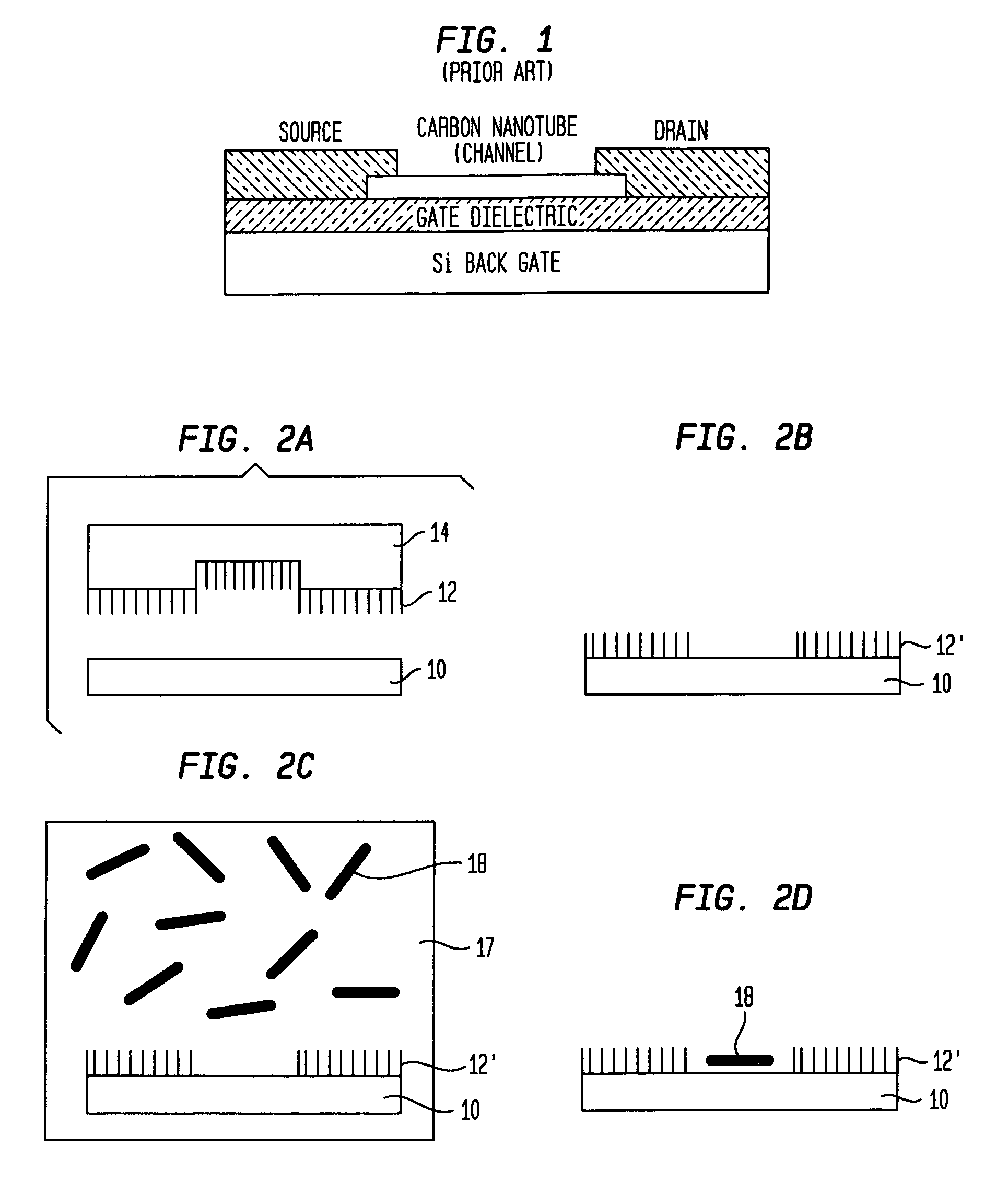
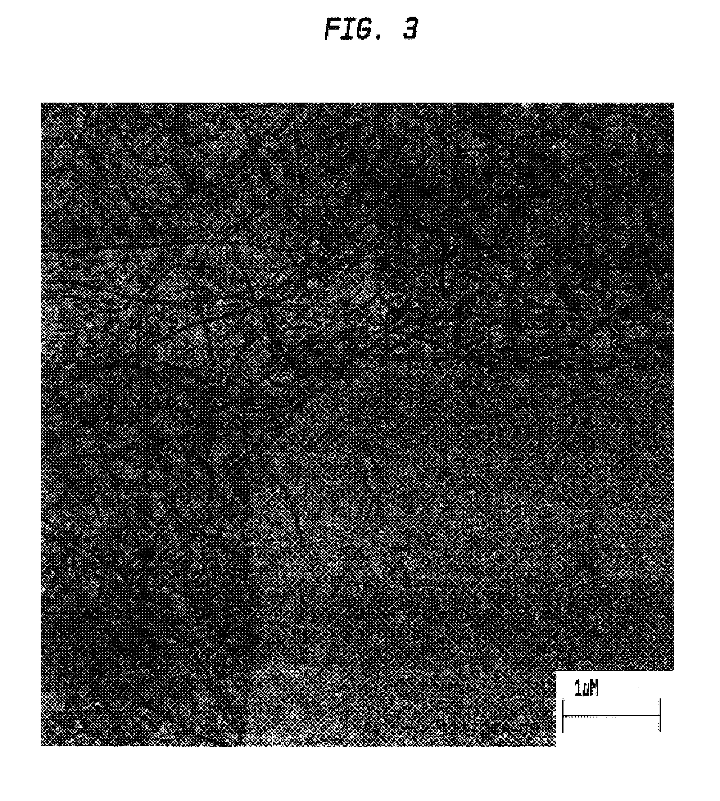
[0045]A silicon wafer was coated with 100 nm of hafnium oxide by vacuum evaporation. A poly(dimethoxysilane) (PDMS) stamp with prepatterned features (indentations) was soaked with a 5 mM solution of hexadecylphosphonic acid in isopropyl alcohol and dried with stream of nitrogen. The PDMS stamp was then pressed against the substrate with hafnium oxide surface and held for few seconds, and then heated at 100° C. for one minute. The stamped substrate was then coated with a dispersion of carbon nanotubes in dichloroethylene and dried under stream of nitrogen. The substrate was then immersed in dichloroethylene and agitated mildly to remove any carbon nanotubes on the stamped area. This process lead to deposition of carbon nanotubes only on area of the substrate which was not stamped (exposed hafnium oxide surface) as shown in FIG. 3. No nanotube formation was observed in the stamped area.

example 2

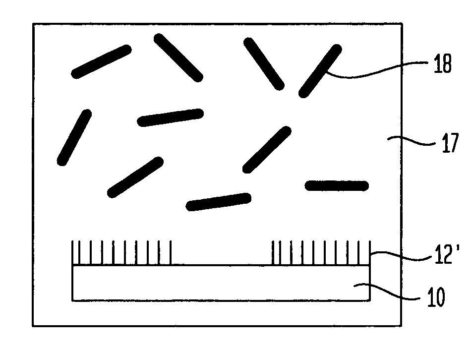
[0046]A silicon wafer with 100 nm of silicon oxide on the surface was patterned with 10 nm of aluminum oxide by evaporation through a shadow mask. The substrate was then immersed in a 5 mM solution of hexadecylphosphonic acid in ethanol. After 2 hours, the substrate was removed from the solution and washed with ethanol and dried at 100° C. for one minute. A dispersion of carbon nanotubes in dichloroethylene was deposited on the substrate and dried under stream of nitrogen. The substrate was then washed with the solvent and dried at room temperature. In this example, carbon nanotubes were deposited on exposed silicon dioxide surface as shown in FIG. 5. In this example, the carbon nanotubes adhered to the cleaned SiO2 surface and not to the treated Al2O3.

example 3

[0047]A silicon wafer with 100 nm of silicon oxide on the surface was patterned, via standard lithography, with a 9 nm aluminum layer. The aluminum layer was then oxidized in an oxygen plasma. The sample was placed in a dilute (4 mM in methanol) 4-aminobutylphosphonic acid (ABPA) solution for several days. The ABPA binds only to the Al2O3 and not to the SiO2. The sample was then placed in a suspension of carbon nanotubes in surfactant Triton-X and water for 4 hours. The substrate was removed from the solution and washed with excess solvent. Examination of the substrate shows that carbon nanotubes were found mainly on the areas where ABPA binds, that is, on the Al2O3 patterned lines (FIG. 7). The surrounding SiO2 showed a very low density of carbon nanotubes or amorphous carbon.


PUM

PropertyMeasurementUnit
thickaaaaaaaaaa
lengthaaaaaaaaaa
lengthaaaaaaaaaa

Abstract

The present invention provides a method for the selective placement of carbon nanotubes on a particular surface. In particular, the present invention provides a method in which self-assembled monolayers formed on an unpatterned or patterned metal oxide surface are used to attract or repel carbon nanotubes from a dispersion containing the same. In accordance with the present invention, the carbon nanotubes can be attracted to the self-assembled monolayers so as to be attached to the metal oxide surface, or they can be repelled by the self-assembled monolayers bonding to a predetermined surface other than the metal oxide surface containing the self-assembled monolayers.

Description

FIELD OF THE INVENTION[0001]The present invention generally relates to the selective placement of carbon nanotubes on a particular surface. More particularly, the present invention provides a method in which self-assembled monolayers formed on a particular surface are used to attract or repel carbon nanotubes from a dispersion containing the same. The present invention also relates to the use of self-assembled monolayers of phosphonic acid on oxide surfaces for the selective placement of carbon nanotubes (CNTs).BACKGROUND OF THE INVENTION[0002]In the field of molecular electronics, few materials show as much promise as carbon nanotubes that comprise hollow cylinders of graphite that have a diameter of a few Angstroms. Nanotubes can be implemented in electronic devices, such as, for example, diodes and transistors, depending on the characteristics of the nanotube. Nanotubes are unique for their size, shape and physical properties. For example, carbon based nanotubes resemble a hexago...

Claims


Application Information

Patent Timeline
Patent Type & Authority Patents(United States)
IPC IPC(8): B05D5/00
CPCB05D1/283B82Y30/00B82Y40/00
Inventor AFZALI-ARDAKANI, ALIHANNON, JAMES BOWLER
Owner GLOBALFOUNDRIES INC
Why Eureka
Try Eureka