Planar split-gate high-performance MOSFET structure and manufacturing method

a technology of metal oxide semiconductor field effect transistor and planar split gate, which is applied in the direction of semiconductor devices, electrical equipment, transistors, etc., can solve the problems of device prone to punching, difficult to precisely control the threshold, and the conventional manufacturing technology of mosfet device with planar gate is still challenged by several technical difficulties and limitations, so as to achieve uniform doping control, improve breakdown, and high electric field

a technology of metal oxide semiconductor field effect transistor and planar split gate, which is applied in the direction of semiconductor devices, electrical equipment, transistors, etc., can solve the problems of device prone to punching, difficult to precisely control the threshold, and the conventional manufacturing technology of mosfet device with planar gate is still challenged by several technical difficulties and limitations, so as to achieve uniform doping control, improve breakdown, and high electric field

US7504676B2Active Publication Date: 2009-03-17ALPHA & OMEGA SEMICON LTD

Image

  • Planar split-gate high-performance MOSFET structure and manufacturing method
  • Planar split-gate high-performance MOSFET structure and manufacturing method
  • Planar split-gate high-performance MOSFET structure and manufacturing method

Examples


Embodiment Construction

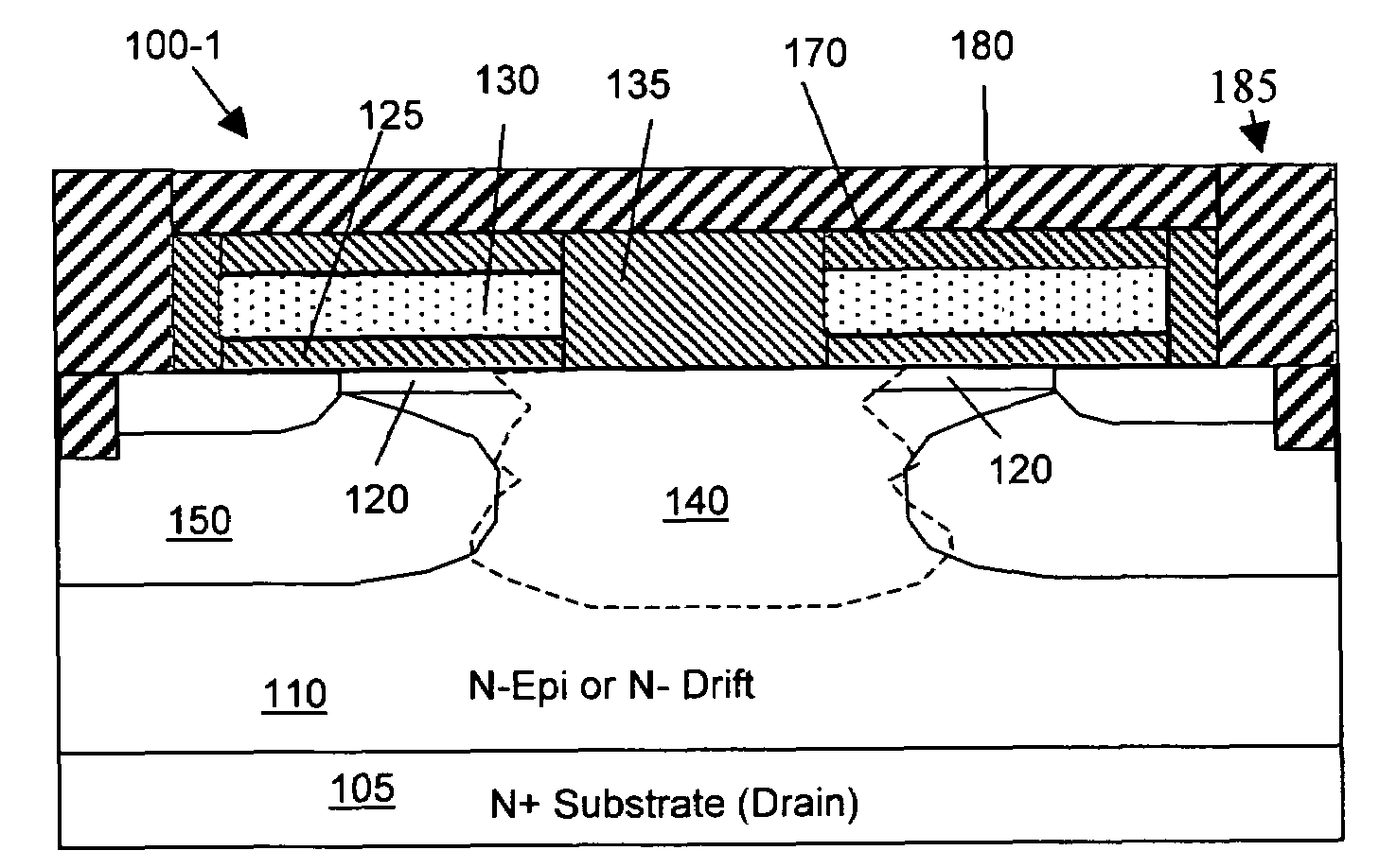
[0031]Referring to FIG. 2A for a cross sectional view of an N-channel MOSFET device 100-1 of this invention. The trenched MOSFET device 100-1 is supported on a substrate 105 formed with an epitaxial layer 110. The MOSFET device 100-1 includes a split gate 130 with a gap opened in the polysilicon gate 130 filled with dielectric material 135. The split gate 130 is disposed above a gate oxide layer 125 formed on top of the epitaxial layer 110. The MOSFET device further includes a shallow surface doped layer 120 immediately below the gate oxide layer 125 to form a channel. In an embodiment, the shallow surface doped region 120 is formed by a blanket low dose implantation such as B+ ion dopant. A vertical and deep JFET diffusion region 140 such as an N+ diffusion region is formed in the epitaxial layer 110 under the gap of the split gate 130. This N+ region 140 counter-dopes the shallow surface doped layer and links the end of channel to the drain by extending from the top surface of epi...


PUM


Abstract

This invention discloses an improved semiconductor power device includes a plurality of power transistor cells wherein each cell further includes a planar gate padded by a gate oxide layer disposed on top of a drift layer constituting an upper layer of a semiconductor substrate wherein the planar gate further constituting a split gate including a gap opened in a gate layer whereby the a total surface area of the gate is reduced. The transistor cell further includes a JFET (junction field effect transistor) diffusion region disposed in the drift layer below the gap of the gate layer wherein the JFET diffusion region having a higher dopant concentration than the drift region for reducing a channel resistance of the semiconductor power device. The transistor cell further includes a shallow surface doped regions disposed near a top surface of the drift layer under the gate adjacent to the JFET diffusion region wherein the shallow surface doped region having a dopant concentration lower than the JFET diffusion region and higher than the drift layer.

Description

BACKGROUND OF THE INVENTION[0001]1. Field of the Invention[0002]The invention relates generally to the semiconductor power devices. More particularly, this invention relates to new device configurations and manufacturing method for a metal oxide semiconductor field effect transistor (MOSFET) device with planar split gate structure to improve device performance.[0003]2. Description of the Prior Art[0004]Even though a semiconductor power device with planar gate structure is more compatible with multiple foundries and can be produced at a lower production cost, however, conventional technologies for manufacturing a metal oxide semiconductor field effect transistor (MOSFET) device with planar gates are still challenged by several technical difficulties and limitations. Specifically, the DMOS process produces a channel with uneven channel doping density as shown in FIG. 1D such that precision control of threshold is difficult and the device is susceptible to punch-through. As shown in FI...

Claims


Application Information

Patent Timeline
17 Mar 2009
Publication
US7504676B2
IPC
H01L29/80
CPC
H01L29/0847; H01L29/0878; H01L29/1095; H01L29/42372; H01L29/42376; H01L29/66712; H01L29/7802; H01L29/7828
Inventors
BHALLA, ANUP; HEBERT, FRANCOIS