Heat dissipating semiconductor package and fabrication method thereof

Inactive Publication Date: 2009-03-24
SILICONWARE PRECISION IND CO LTD
View PDF14 Cites 12 Cited by
  • Summary
  • Abstract
  • Description
  • Claims
  • Application Information

AI Technical Summary

Benefits of technology

[0027]It should be noted that, in the heat dissipating semiconductor package and the fabrication method thereof according to the present invention, the chip carrier and the electrical connection method between the semiconductor chip and the chip carrier can be selected to have various combinations and various modifications, without departing from the scope and spirit of the present invention. Therefore, according to the heat dissipating semiconductor package and the fabrication method thereof in the present invention, a semiconductor chip is mounted on and electrically connected to a chip carrier, and a heat sink is mounted on the semiconductor chip, wherein the heat sink includes an insulating core layer, thin metallic layers provided on upper and lower surfaces of the insulating core layer, and at least one thermal via hole. Then, a molding process is performed to completely encapsulate the semiconductor chip on the chip carrier and the heat sink with an encapsulant to form a package unit. Subsequently, a singulation process is performed to remove peripheral non-electrical portions of the package unit after completing the molding process. A part of the encapsulant above the thin metallic layer on the upper surface of the heat sink is removed, such that the thin metallic layer on the upper surface of the heat sink is exposed. During the singulation process, the cutting tool is moved to cut the insulating co

Problems solved by technology

The highly integrated semiconductor chip during operation usually produces a large amount of heat.
As the semiconductor chip is encapsulated by an encapsulant that is made of a resin material having poor thermal conductivity (a coefficient of thermal conductivity thereof is only 0.8 w/m-k), the heat produced from the semiconductor chip cannot be effectively dissipated through the encapsulant.
This results in unsatisfactory heat dissipating efficiency and adversely affects the performance and lifetime of the semiconductor chip.
However, the semiconductor package 1 causes significant drawbacks during fabrication thereof.
However, if the top surface 11a of the heat sink 11 fails to effectively abut against the top wall of the mold cavity, resin flashes of the encapsulant 12 are formed on the top surface 11a of the heat sink 11, which not only deteriorate the heat dissipating efficiency but also impair appearance of the fabricated product.
In such case, an additional deflashing process is usually required to remove the flashes, which undesirably prolongs the fabrication time, increases fabrication costs, and possibly damages the fabricated product.
On the other hand, too close contact between the heat sink 11 and the top wall of the mold cavity may lead to cracking of the

Method used


Image

  • Heat dissipating semiconductor package and fabrication method thereof
  • Heat dissipating semiconductor package and fabrication method thereof
  • Heat dissipating semiconductor package and fabrication method thereof

Examples


first embodiment

[0041]FIGS. 4A to 4F show procedural steps of a fabrication method of a heat dissipating semiconductor package according to a first embodiment of the present invention.

[0042]As shown in FIGS. 4A and 4B, an array-type chip carrier module plate such as a substrate module plate 40A is provided, which includes a plurality of chip carriers such as substrates 40 arranged in an array. Each of the substrates 40 comprises an upper surface 400, a lower surface 401, and a through hole 402 formed therein. It should be noted that, in addition to being arranged in an array, the substrates 40 may also be arranged in a strip, or the fabrication method may be performed using a single substrate under appropriate process conditions.

[0043]Then, an active surface 41a of a semiconductor chip 41 is mounted at a predetermined position on the upper surface 400 of each of the substrates 40 by an adhesion layer 45 such as silver paste, with one end of the through hole 402 of each of the substrates 40 being se...

second embodiment

[0049]FIGS. 5A to 5G show procedural steps of a fabrication method of a heat dissipating semiconductor package according to a second embodiment of the present invention. The fabrication method of the second embodiment is similar to that of the first embodiment, with a primary difference in that a semiconductor chip in the second embodiment is mounted on and electrically connected to a substrate by a flip-chip method.

[0050]As shown in FIGS. 5A and 5B, an array-type chip carrier module plate such as a substrate module plate 50A is prepared, which includes a plurality of chip carriers such as substrates 50 arranged in an array. Each of the substrates 50 comprises an upper surface 500 and a lower surface 501. It should be noted that, in addition to being arranged in an array, the substrates 50 may also be arranged in a strip, or the fabrication method may be performed using a single substrate under appropriate process conditions.

[0051]Next, an active surface 51a of a semiconductor chip ...

third embodiment

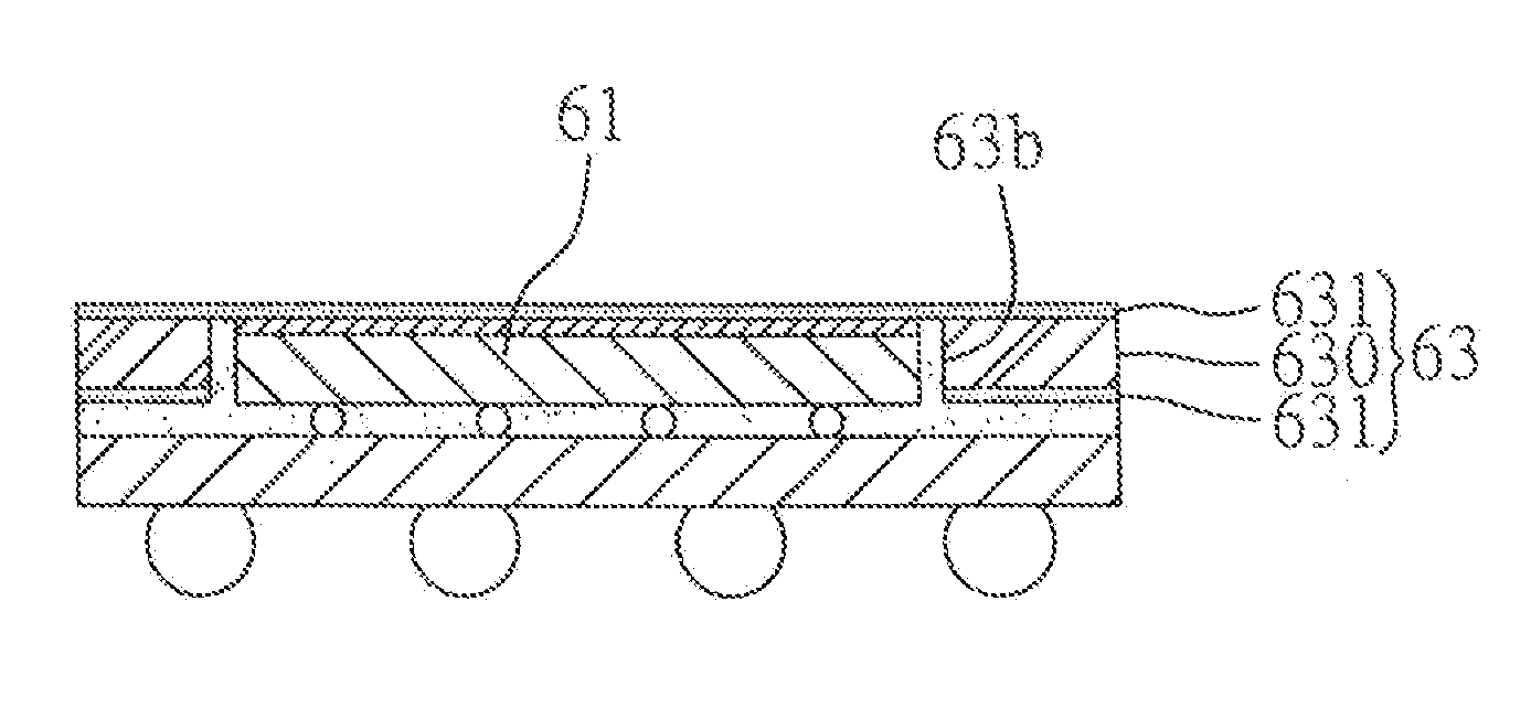
[0057]FIG. 6 shows a cross-sectional view of a semiconductor package according to a third embodiment of the present invention. The semiconductor package of third embodiment is fabricated by a method similar to the fabrication methods in the first and second embodiments, with a primary difference in that in the third embodiment, a heat sink 63 attached to a semiconductor chip 61 is formed with an opening 63b at a position corresponding to the chip 61. Particularly, a part of an insulating core layer 630 and a part of a thin metallic layer 631 on a lower surface of the heat sink 63 corresponding in position to the chip 61 are removed to thereby form the opening 63b via which a part of a thin metallic layer 631 on an upper surface of the heat sink 63 is exposed. When attaching the heat sink 63 to the chip 61, the chip 61 can be received in the opening 63b, thereby further reducing the height of the semiconductor package. Moreover, a non-active surface of the chip 61 is in contact with ...


PUM

PropertyMeasurementUnit
Electrical conductoraaaaaaaaaa

Abstract

A heat dissipating semiconductor package and a fabrication method thereof are provided. A semiconductor chip is mounted on a chip carrier. A heat sink is mounted on the chip, and includes an insulating core layer, a thin metallic layer formed on each of an upper surface and a lower surface of the insulating core layer and a thermal via hole formed in the insulating core layer. A molding process is performed to encapsulate the chip and the heat sink with an encapsulant to form a package unit. A singulation process is performed to peripherally cut the package unit. A part of the encapsulant above the thin metallic layer on the upper surface of the heat sink is removed, such that the thin metallic layer on the upper surface of the heat sink is exposed, and heat generated by the chip can be dissipated through the heat sink.

Description

FIELD OF THE INVENTION[0001]The present invention relates to heat dissipating semiconductor packages and fabrication methods thereof, and more particularly, to a semiconductor package with a heat sink and a method for fabricating the semiconductor package.BACKGROUND OF THE INVENTION[0002]Ball Grid Array (BGA) packaging technology, which is a well-known advanced technology in the relevant art, is performed in a manner as to mount a semiconductor chip on a front side of a substrate and implant a grid array of solder balls on a back side of the substrate. The solder balls are used to electrically connect the entire package unit to an external printed circuit board. The BGA packaging technology advantageously incorporates more I / O (input / output) connections within the same unit area of a chip carrier (e.g. the substrate) such that the high integration requirement of the semiconductor chip is satisfied.[0003]The highly integrated semiconductor chip during operation usually produces a lar...

Claims


Application Information

Patent Timeline
IPC IPC(8): H01L23/34H01L23/10
CPCH01L21/4871H01L21/561H01L23/3107H01L23/3128H01L23/367H01L23/3677H01L23/3733H01L23/4334H01L23/49816H01L24/97H01L23/49548H01L2224/16225H01L2224/48091H01L2224/4824H01L2224/73215H01L2224/73253H01L2224/73265H01L2224/97H01L2924/01013H01L2924/01029H01L2924/01047H01L2924/01074H01L2924/01079H01L2924/01082H01L2924/15311H01L24/48H01L2924/01019H01L2924/01024H01L2924/01033H01L2224/16245H01L2224/32225H01L2224/48227H01L2224/32245H01L2224/48247Y10T29/49126H01L2224/85H01L2924/00014H01L2224/81H01L2224/83H01L2924/00H01L2924/00012H01L2924/351H01L24/73H01L2224/45099H01L2224/45015H01L2924/207
Inventor HUANG, CHIEN-PINGHUANG, CHIH-MING
Owner SILICONWARE PRECISION IND CO LTD
Why Eureka
Try Eureka