
Low cost antenna array fabrication technology

a fabrication technology and low cost technology, applied in the field of microwave antenna elements fabrication, can solve the problems that the above-described photoresist methodology is not suitable for high-volume production of small antenna arrays, and achieve the effect of simple and cost-effective methods

Active Publication Date: 2009-03-31
GENERAL ELECTRIC CO
View PDF18 Cites 0 Cited by
  • Summary
  • Abstract
  • Description
  • Claims
  • Application Information

AI Technical Summary

Benefits of technology

"The present invention provides a simple and cost-effective method for producing large volumes of small antenna arrays, such as microwave antenna arrays. The invention involves creating an antenna array pattern as a computer file, printing the pattern onto a transfer paper, and then transferring the printed image onto the surface of a substrate material to be etched. The transferred printed image acts as a mask during etching, and then is removed to reveal the unetched surface that was protected by the mask. The invention also includes an apparatus for carrying out the method. The technical effects of the invention include the ability to produce large volumes of small antenna arrays quickly and efficiently."

Problems solved by technology

However, known methods such as the above-described photoresist methodology are not suitable for high-volume production of small antenna arrays, due to the complexity and labor-intensive steps involved.

Method used


Image

  • Low cost antenna array fabrication technology
  • Low cost antenna array fabrication technology
  • Low cost antenna array fabrication technology

Examples


examples

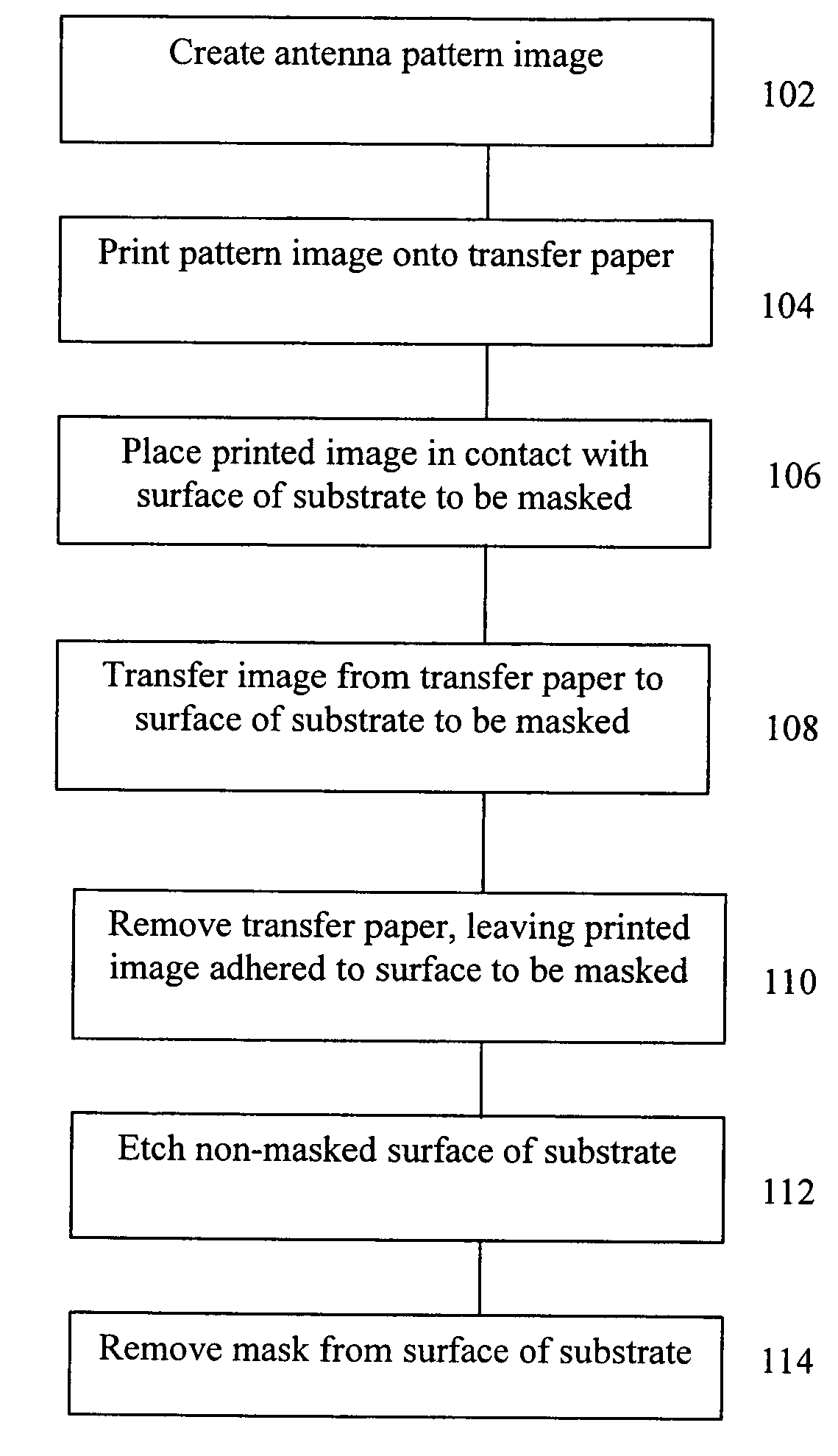
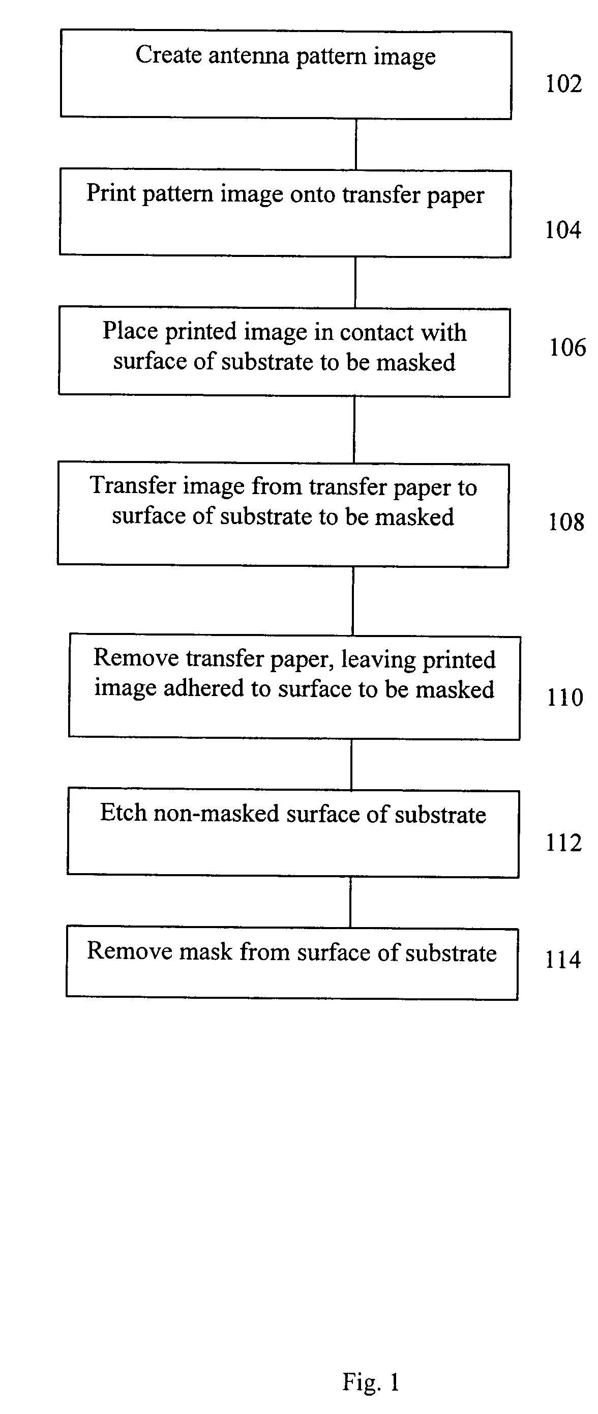
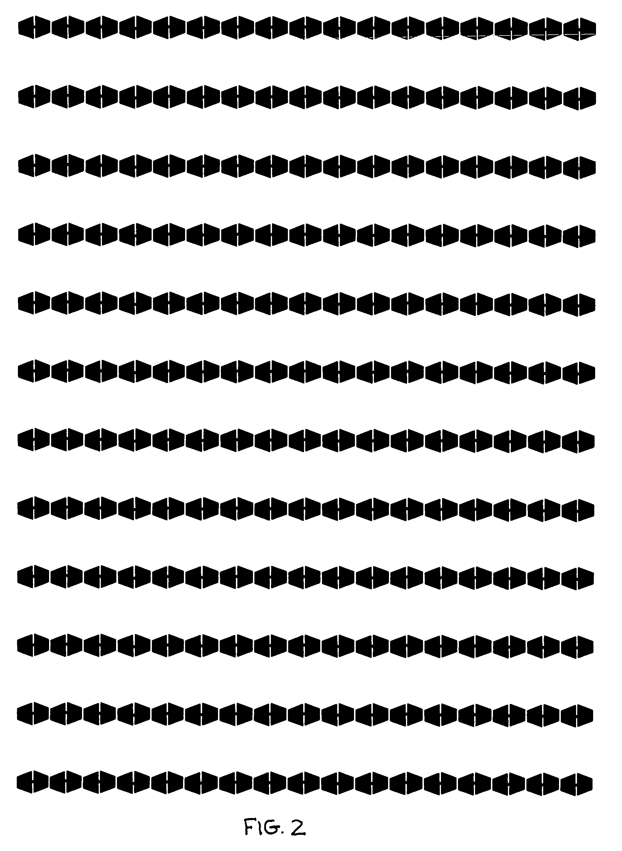
[0019]The methods of the present invention have been found compatible with the etching of antenna arrays onto copper clad kapton, as well as onto copper clad circuit board material. For example, in one embodiment, the exemplary antenna array pattern image of FIG. 1 was created as an AUTOCAD® file on a microprocessor controlled computer. The created pattern image was then saved into memory where it was recalled and sent to a printer for printing as a printed image onto a suitable transfer paper. In this example, the printer used was an Hewlett-Packard Laser Jet 2300 dn, with standard ink as provided in commercially available Hewlett-Packard ink cartridge model Q2610A. The transfer paper used was DECAFIX® brand transfer paper. DECAFIX® is the trademark for decalcomania papers, particularly proprietary transfer papers of the waterslide variety. The DECAFIX® trademark is believed to be owned by Brittains Tullis Russell, Inc. Corporation, with a business address of 500 Summer Street, Sta...


PUM

PropertyMeasurementUnit
pressureaaaaaaaaaa
vacuum pressureaaaaaaaaaa
areaaaaaaaaaaa

Abstract

Methods are provided for producing large volumes of small antenna arrays. In one embodiment, the method comprises the steps of creating an antenna array pattern as a computer file, printing the created pattern onto the surface of a suitable transfer paper, placing the printed image surface in contact with the surface of a material to be etched, and transferring the printed image to the surface of the material to be etched. The transfer can be effected by any combination of chemicals, heat, and / or pressure. After transfer of the printed image, the transfer paper is removed. The step of removing the transfer paper optionally includes wetting the transfer paper in a manner that dissolves the transfer paper leaving the printed antenna pattern on the surface of the material to be etched. The method further includes the step of etching the non-printed portions of the material, preferably by chemical etching, and removing the printed pattern from the surface of the material to yield an antenna array comprising a non-etched portion of the substrate surface. Arrays, and substrates having an etch-resistant mask for making the arrays, are also provided.

Description

FIELD OF THE INVENTION[0001]The present invention is directed to fabrication of microwave antenna elements, and particularly to fabrication of such antenna arrays, such as for use in aircraft applications.BACKGROUND OF THE INVENTION[0002]It is known that antenna arrays have a wide range of applications. They are commonly used in items as diverse as cell phones, aircraft radio and radar systems. Antenna arrays are used to provide directional transmission of an electromagnetic signal as well as to enhance electronic signal recognition. It is known to incorporate antenna arrays into aircraft components, such as microwave antenna arrays. Such arrays can be incorporated into the external surfaces of aircraft assemblies, such as, for example, the fuselage, wings, tail, and other low temperature assemblies.[0003]Known methods to produce antenna arrays utilize photoetching technology. Exemplary prior art methods of photoetching are briefly described U.S. Pat. No. 6,083,767, for example. In ...

Claims


Application Information

Patent Timeline
Patent Type & Authority Patents(United States)
IPC IPC(8): B44C1/22G03F1/92
CPCH01Q1/28H01Q21/0087H05K3/061Y10S428/914H05K2203/0537Y10T428/24802H05K2203/0531
Inventor STOWELL, WILLIAM RANDOLPHSTEELE, MICHAEL R.RENTZ, THOMAS WALTER
Owner GENERAL ELECTRIC CO
Learn More