Method for producing a spiral inductance on a substrate, and a device fabricated according to such a method

a technology of spiral inductance and substrate, which is applied in the manufacture of inductances/transformers/magnets, transformers/inductance coils/windings/connections, etc., can solve the problems of substrate loss, performance loss in regard to resonance frequency and quality factor, and low quality factor relative low, so as to achieve simple and cost-effective method, reduce electrical losses, and simple grounding

Active Publication Date: 2005-11-10
ATMEL CORP
View PDF10 Cites 8 Cited by
  • Summary
  • Abstract
  • Description
  • Claims
  • Application Information

AI Technical Summary

Benefits of technology

[0020] It is therefore the object of the present invention to provide a method for producing a micro-shielded spiral inductance and a device having a spiral inductance that is fabricated in accordance with such a method, which eliminates the aforementioned disadvantages and in particular ensures a simpler and more cost-effective method as well as a device having lower electrical losses and simpler grounding.
[0021] The present invention is based on the idea that an improved integration of the individual metallizations and windings of the spiral inductance, and a direct connection of the upper and lower ground metallizations as well as an increased thickness of the windings of the spiral inductance, the thickness being fabricated in a simple manner, is ensured by the following steps: Forming a structured inductance metallization and a structured upper ground metallization on the top side of a substrate; forming a second dielectric insulating layer at least between the inductance metallization and the upper ground metallization and over the inductance metallization; complete back-etching of a substrate area below the inductance metallization such that at least the windings of the inductance metallization are freely suspended over the completely back-etched area of the substrate, being completely supported by embedding in the insulation layer; and structured metallization of the surface of the back-etched area of the substrate to form an end-to-end connected ground point and of the segments of the inductance metallization located over the completely back-etched area to form windings of the spiral inductance with increased thickness.
[0022] In this way, a spiral inductance can be constructed using a simple and cost-effective production method, whereby the windings are totally shielded from external influences without additional covering and are entirely decoupled from the substrate such that no electromagnetic coupling with the substrate and, therefore, with other devices can occur. Interferences, electromagnetic losses, substrate losses etc. can thereby be reduced or completely eliminated.

Problems solved by technology

General problems with integrated inductances are the relative low quality factors, obtaining a satisfactory grounding, deviating characteristics depending on the substrate geometry, electromagnetic couplings between inductances and the substrate, and relatively low self-resonance frequencies.
However, production costs, integration density, and reliability are additional deciding factors, which have to be considered in the production of integrated inductances.
The problem in general is, therefore, that an integration of planar spiral inductances on, for example, a silicon substrate, usually results in performance losses in regard to the resonance frequency and the quality factor.
Primarily, the coupling between the spiral inductance and its surrounding area over the silicon substrate, and the lack of a good earth plane due to substrate losses is the cause of such disadvantages of the integrated spiral inductances.
In addition, the magnetic flow along the coil, which is directed vertically into the substrate, also causes substrate losses due to the generated eddy currents.
These effects also reduce the quality factor of the integrated planar spiral inductance.
However, this is relatively difficult to do.
However, this approach has the disadvantage that high coupling, that is, substrate losses occur.
This, however, requires a relatively elaborate procedure.
The disadvantage thereby is that substantial substrate losses occur.
The disadvantage of this conventional approach has proven to be the fact that the production process is very complicated, expensive, and time-consuming.

Method used


Image

  • Method for producing a spiral inductance on a substrate, and a device fabricated according to such a method
  • Method for producing a spiral inductance on a substrate, and a device fabricated according to such a method
  • Method for producing a spiral inductance on a substrate, and a device fabricated according to such a method

Examples


first embodiment

[0052]FIGS. 7a to 7m illustrate cross-sectional views of an exemplary device in selected method modes, whereby with reference to FIGS. 7a to 7m, a production method for a device having a spiral inductance on a substrate according to the present invention is described in detail.

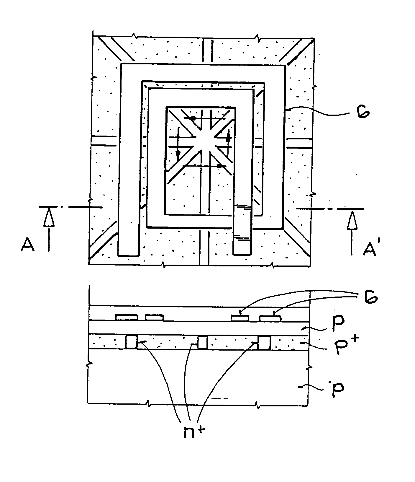
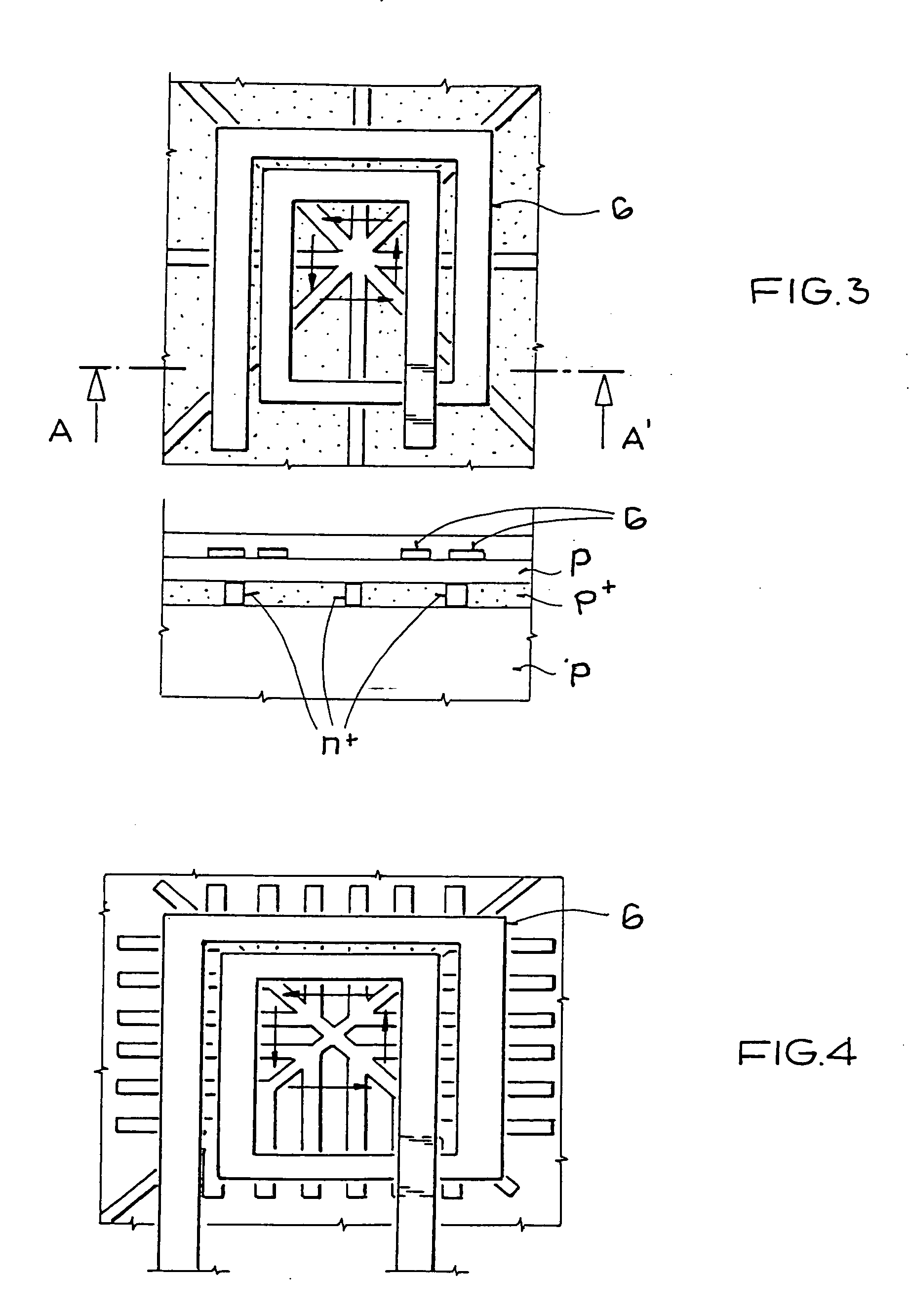
[0053] As is shown in FIG. 7a, for example, in a step for the fabrication of metallizations, the top and bottom sides of a substrate 1 are coated with a first layer, for example, a first dielectric insulating layer 2, that is, a further dielectric insulating layer 4 (henceforth referred to as third insulating layer 4). However, in certain instances, layers 2 and 4 can also be omitted. The substrate 1 is, for example, a low-resistance silicon semiconductor substrate, or the like. Both the first and the third dielectric insulating layer 2, or 4, can be formed, for example, as an approximately 1-2 μm-thick silicon nitride or silicon dioxide layer. Subsequently, an inductance metallization 6 and an upper ground me...

fourth embodiment

[0081]FIG. 11 illustrates a cross-sectional view of a device according to the present invention. As is shown in FIG. 11, a covering metallization 16 is additionally formed over the spiral inductance, whereby the rim areas of the covering metallization 16 are respectively connected with the upper ground metallization. The covering metallization 16 can be deposited by using a thick additional photoresist layer on the top side of the instant device. After a structuring of the SU-8 membrane 3 (again, preferably done during the application of the SU-8 layer), a thick photoresist layer, for example, about 30 μm thick, is deposited on the second dielectric insulating layer 3, and structured. Preferably, the sharp corners of the additional photoresist material can be smoothened, for example, by using an oxygen-plasma etching procedure. Thereafter, the shape of the covering metallization can be formed as a shield from external soiling and interferences by applying a standard metallization pr...


PUM

PropertyMeasurementUnit
inductanceaaaaaaaaaa
thickaaaaaaaaaa
spiral inductanceaaaaaaaaaa

Abstract

A device and a method for producing such a device is provided, whereby the windings of a spiral inductance are embedded in a membrane such that they are freely suspended over a completely back-etched area of the substrate for a decoupling of the windings from the substrate. An additional substrate is connected to the bottom side of the back-etched area of the processed substrate such that a hollow cavity is formed for a decoupling of the windings from the substrate.

Description

[0001] This nonprovisional application claims priority under 35 U.S.C. § 119(a) on German Patent Application No. DE 102004022139.1, which was filed in Germany on May 5, 2004, and which is herein incorporated by reference. BACKGROUND OF THE INVENTION [0002] 1. Field of the Invention [0003] The present invention relates to a method for producing a spiral inductance on a substrate and a device that is fabricated in accordance with such the method. [0004] 2. Description of the Background Art [0005] With increasing operating frequency, device modeling for devices that are integrated on a semiconductor substrate is playing an increasingly bigger role because it causes transmission-line properties, reflections on discontinuities, overlapping and dissipations to increase. Thus, taking these effects into consideration in modeling, particularly in the high frequency field, is generally a must. In particular, in a low-resistance substrate, for example a silicon substrate of a silicon-germanium...

Claims


Application Information

Patent Timeline
Patent Type & Authority Applications(United States)
IPC IPC(8): H01F17/00H01F41/04H01L21/02H01L21/764H01L23/522H01L23/64H01L27/08
CPCH01F17/0006H01F41/041H01F2017/0046H01F2017/008H01L21/764H01L23/5227H01L27/08H01L28/10H01L2924/0002H01L2924/00
Inventor JOODAKI, MOJTABA
Owner ATMEL CORP
Why Eureka
Try Eureka