

Lithographic projection apparatus and a device manufacturing method
a technology of lithographic projection and manufacturing method, applied in the direction of optical devices, photomechanical devices, instruments, etc., can solve the problems of rotating asymmetric optical aberration and severely degrade the device pattern image, and achieve the effect of reducing the problem of astigmatism aberration
- Summary
- Abstract
- Description
- Claims
- Application Information
AI Technical Summary
Benefits of technology
Problems solved by technology
Method used
Image

Examples
Embodiment Construction
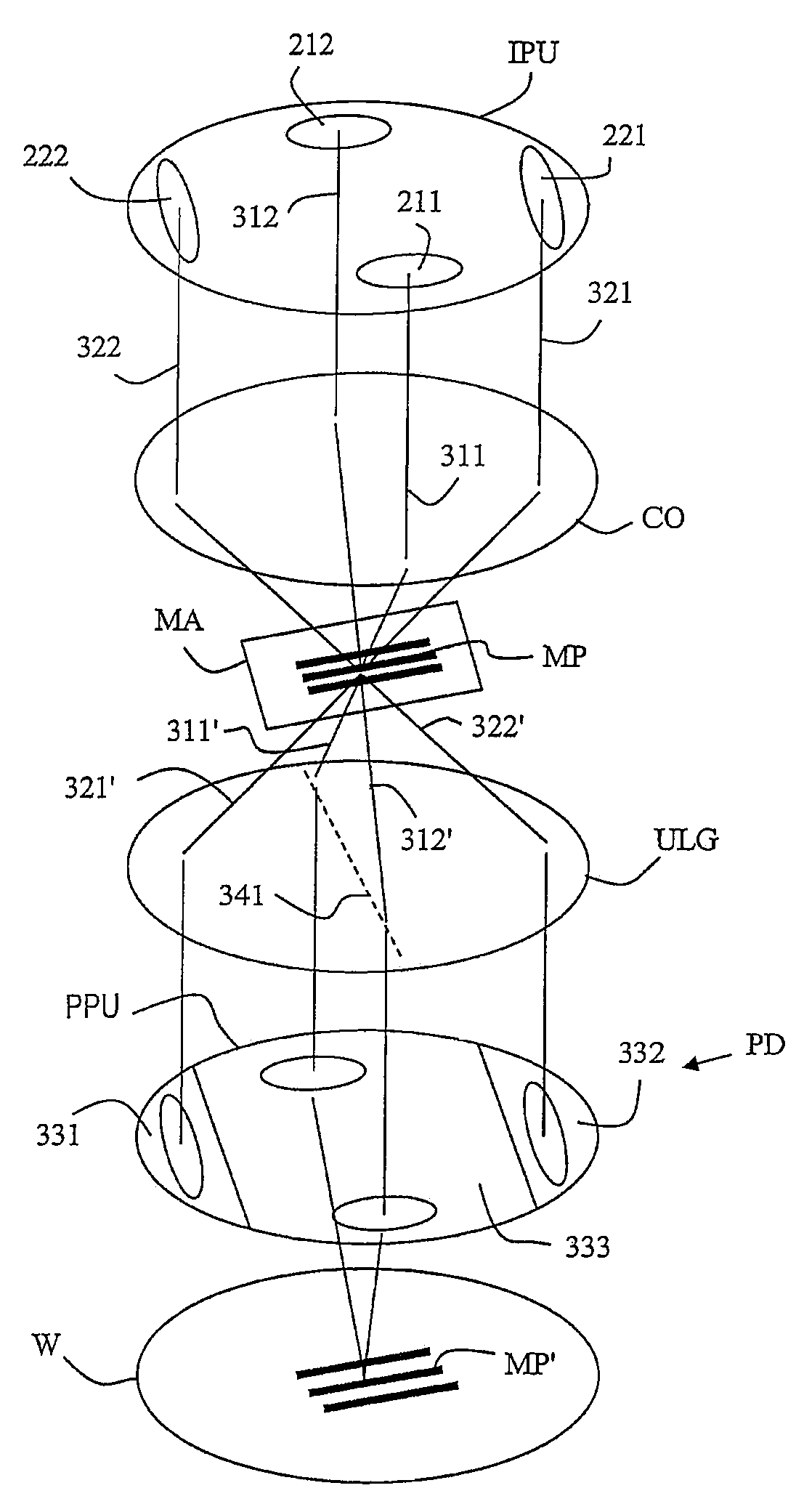
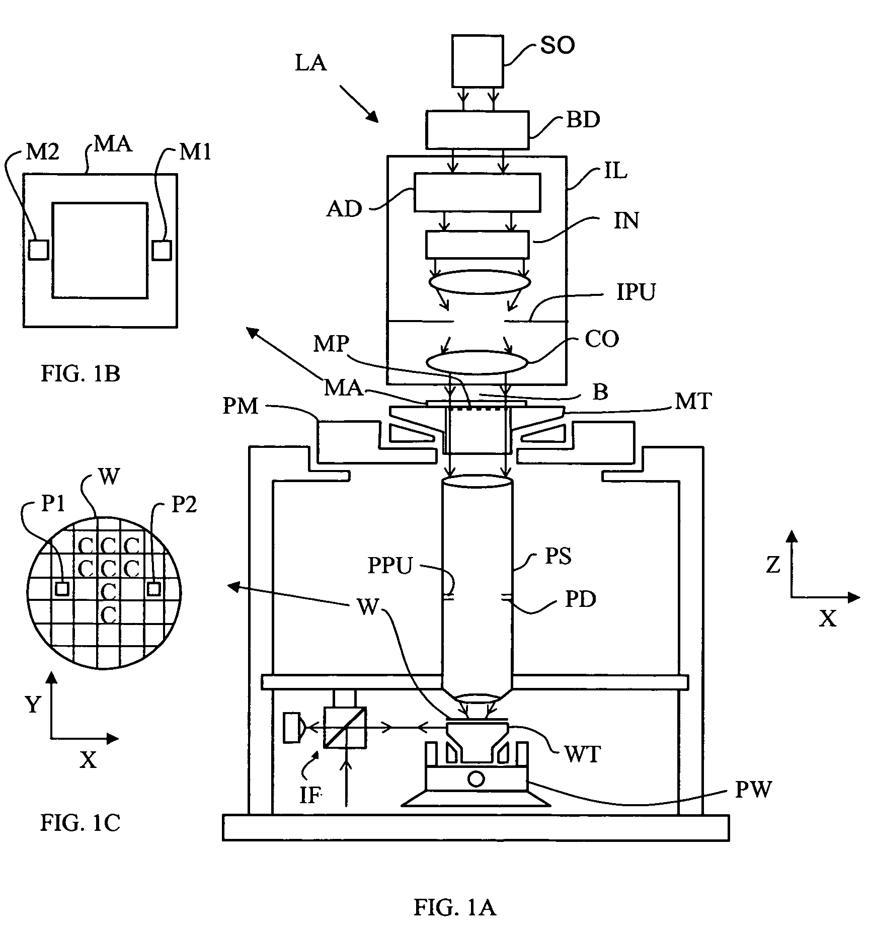
[0021]FIGS. 1A, 1B and 1C depict a lithographic apparatus LA, a patterning device MA, and a substrate W, according to a first embodiment of the invention. The apparatus LA of FIG. 1A includes an illumination system IL, a support structure (e.g., a mask table) MT, a substrate table (e.g., a wafer table) WT, and a projection system (e.g., a refractive projection lens system) PS.
[0022]The illumination system IL is configured to condition a radiation beam B (e.g., a beam of UV radiation as provided by a mercury arc lamp, or a beam of DUV radiation generated by a KrF excimer laser or an ArF excimer laser). The support structure (e.g., a mask table) MT is constructed to support the patterning device (e.g., a mask) MA having a mask pattern MP and connected to a first positioner PM. The first positioner PM can be configured to accurately position the patterning device in accordance with certain parameters.
[0023]The substrate table (e.g., a wafer table) WT is constructed to hold a substrate ...
PUM
 Abstract
Description
Claims
Application Information