

DRAM layout with vertical FETs and method of formation
a vertical cell and capacitor technology, applied in the field of memory cell arrays, can solve the problems of cross-point cells, difficult to fabricate, and high cost of cross-point cells, and achieve the effect of solving integration problems of vertical cell drams using stacked capacitors
- Summary
- Abstract
- Description
- Claims
- Application Information
AI Technical Summary
Benefits of technology
Problems solved by technology
Method used
Image

Examples
first embodiment
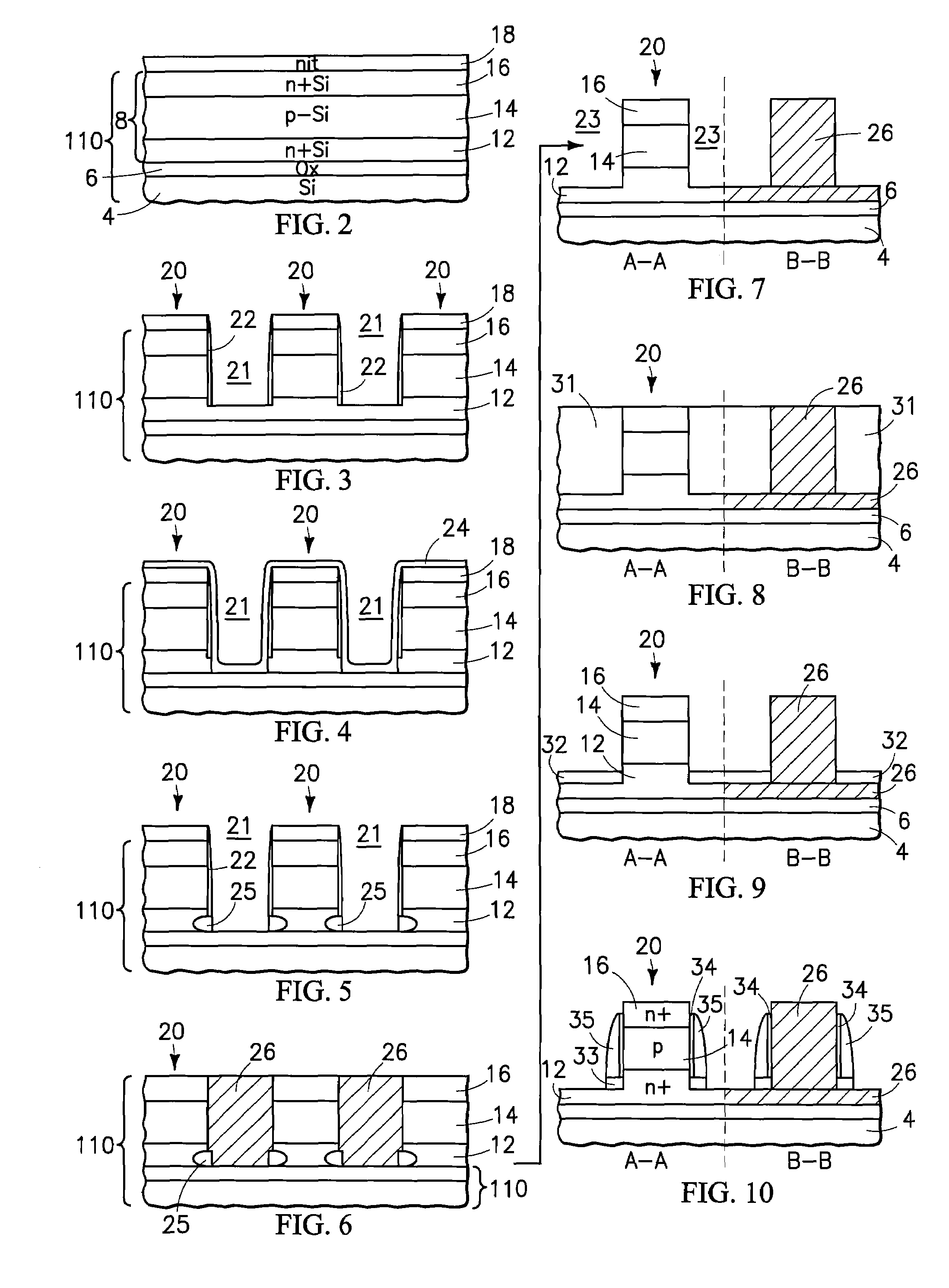
[0073]Subsequent to the formation of the first set of trenches 21, a second set of trenches 23 (FIG. 17) are formed by directional etching, for example, as explained above with reference to FIGS. 7-10. The second set of trenches are then filled with an insulating material, preferably an oxide material such as silicon oxide, which is etched back by known methods in the art to form an oxide layer similar to oxide layer 32 of FIG. 9. Subsequent to the formation of the oxide layer (which will be etched to form oxide regions 33 of FIG. 17), a thin gate oxide layer 34 and a gate electrode 35 are sequentially formed on the sidewalls of the stacks 20, as shown in FIG. 17. The thin gate oxide layer 34 and word lines or gate electrodes 35 (FIG. 17) of the vertical transistors 290 (FIG. 18) are formed as described above with reference to the formation of the word lines or gate electrodes of the present invention. The thin gate oxide layer 34, which will act as a gate insulator layer, may compr...
fourth embodiment
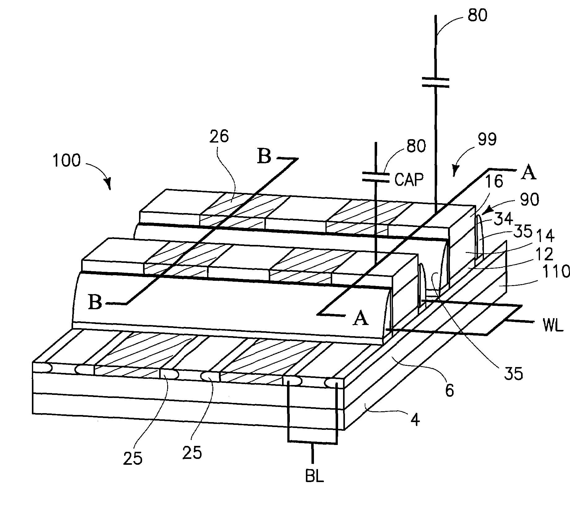
[0076]FIGS. 20-29 illustrate the present invention, according to which device array 400 (FIG. 29) comprises a plurality of DRAM cells 499, each DRAM cell 499 comprising two devices, a vertical transistor 490 and a capacitor 80 located above the transistor 490. Vertical transistor 490 of the device array 400 comprises buried bit lines 25 disposed adjacent a gate stack comprising epitaxial layers 414, 416, 418, and not doped silicon layers as in the previously-described embodiments.
[0077]FIG. 20 illustrates a SOI substrate 110 similar to that shown in FIG. 2. As in the above-described embodiments, the SOI substrate 110 may be formed by a bonding and etching back method, according to which a silicon substrate 4 is thermally oxidized to grow a layer of silicon oxide 6 with a thickness of about 1 micron. Subsequently, an n-type single crystalline silicon substrate 8 is opposed to the silicon oxide layer 6, and the silicon substrate 4, with the oxide layer 6, is then contacted with the cr...
fifth embodiment
[0086]FIGS. 30-36 illustrate the present invention, according to which epitaxial silicon layers 414, 416, 418 are formed as part of stack 420 provided over a p-type silicon wafer 210, and not over a SOI substrate, such as the SOI substrate 110 described above. As in the previously-described embodiment with reference to FIGS. 20-29, epitaxial silicon layers 414, 416, 418 are formed as part of stack 420 subsequent to the formation of the silicide bit lines 25 of FIG. 33, and as part of DRAM cells 599 of device array 500 (FIG. 36).
[0087]Accordingly, FIG. 30 illustrates the formation of an n+ silicon layer 12 and a thick insulating layer 51 of about 2,000 Angstroms to about 10,000 Angstroms, which are formed over the p-type silicon wafer 210 by chemical vapor deposition (CVD) or other suitable methods, for example. The n+ silicon layer 12 may be also formed by appropriately doping a top portion of the p-type silicon wafer 210, as explained above with reference to the previously describe...
PUM
 Abstract
Description
Claims
Application Information