Semiconductor device and its manufacturing method

a technology of semiconductor devices and manufacturing methods, applied in semiconductor devices, semiconductor/solid-state device details, electrical apparatus, etc., can solve problems such as ineffective connection plugs, changes with time, and electrical interferen

Inactive Publication Date: 2009-04-14
NEC CORP
View PDF13 Cites 21 Cited by
  • Summary
  • Abstract
  • Description
  • Claims
  • Application Information

AI Technical Summary

Benefits of technology

[0014]According to the present invention, it is possible to provide a semiconductor device having an interconnection structure resistant to electromigration and stress migration.

Problems solved by technology

Electromigration and stress migration pose problems, such as changes with time in the resistance of metal interconnections and connection plugs and disconnections of them.
In this case, the disconnection of interconnections can be prevented by the redundancy effect of the interconnection material B. However, this method is effective for interconnections although it is not effective for connection plugs.
Also, although interconnections do not lead to disconnections, there is a problem that the interconnection resistance increases.
Furthermore, this method is not effective for stress migration.
When methods that involve combining interconnection materials are adopted, it is impossible to prevent the occurrence of voids due to the electromigration in connection plugs.
Also, in interconnections, it is impossible to prevent changes in resistance that are caused of the disconnection of part of the interconnections due to electromigration or stress migration.
However, the reason why connection plugs formed from multilayer carbon nanotubes have high resistance values in spite of the fact that the multilayer carbon nanotubes have metallic properties and low resistance is that the contact resistance between the carbon nanotubes and the metal interconnections is high, with the result that the resistance of connection plugs increases due to the contact resistance even when the resistance of the carbon nanotubes is low.

Method used


Image

  • Semiconductor device and its manufacturing method
  • Semiconductor device and its manufacturing method
  • Semiconductor device and its manufacturing method

Examples


first embodiment

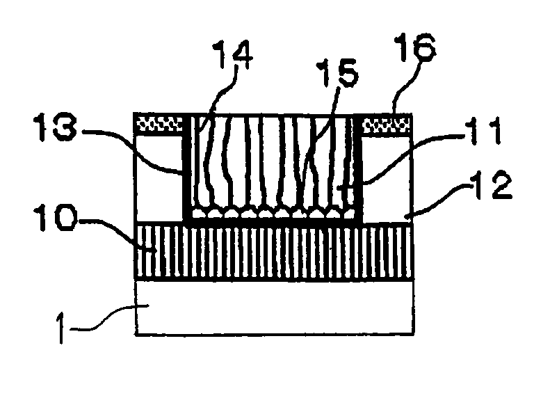
[0051]The description will be given by using FIG. 1 that is a schematic sectional view of an interconnection structure in a semiconductor device of the first embodiment.

[0052]In FIG. 1, an interconnection 11 is constituted by a metal layer 39, which is formed on an insulating film 10 formed on a semiconductor substrate 1 on which a device element or an interconnection is formed. Carbon nanotubes 14 are mixed in the metal layer 39 which constitutes the interconnection 11. The carbon nanotube 14 is formed on a particle 15 of nickel formed on the insulating film 10. The particle 15 acts as a catalyst during the growth of the carbon nanotube, and the carbon nanotube 14 grows, with the particle 15 serving as a nucleus.

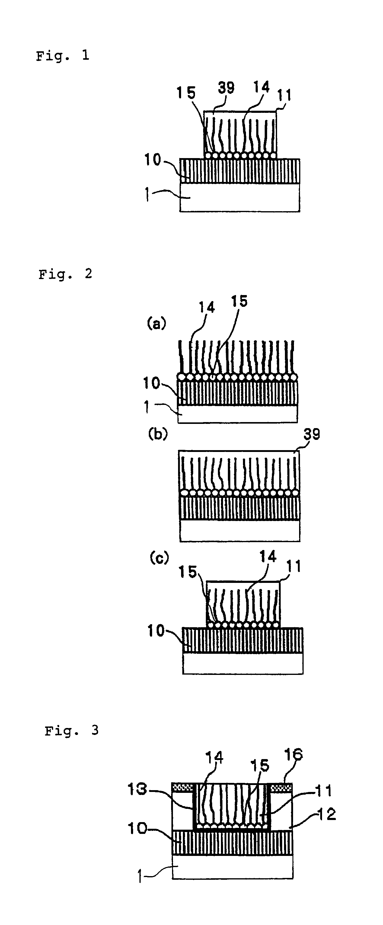
[0053]A manufacturing method of a semiconductor device of the first embodiment will be described with reference to FIGS. 2(a) to 2(c).

(Formation of Substrate and Formation of Carbon Nanotubes)

[0054]The insulating film 10 is formed on a silicon substrate 1 on which a semicon...

second embodiment

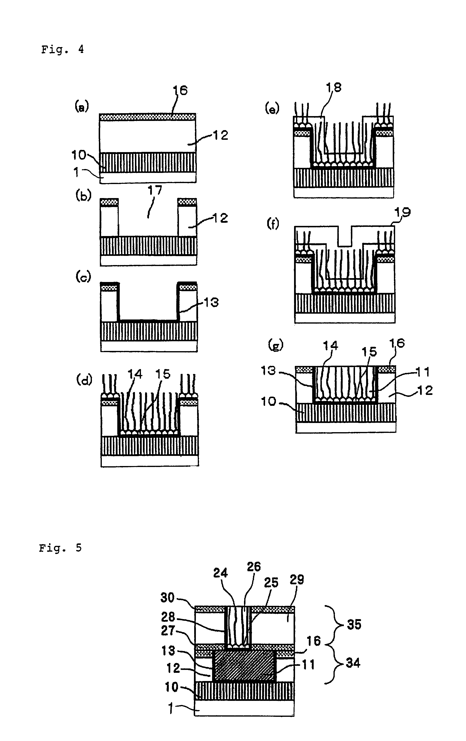
[0079]The second embodiment of the present invention is an interconnection trench structure by the single damascene process.

[0080]FIG. 3 shows an interconnection structure by the single damascene process.

[0081]The interconnection structure by the single damascene process will be described. There are formed an insulating film 10, which is formed on a semiconductor substrate 1 on which a device element or an interconnection is formed, an interlayer dielectric film 12 formed on the insulating film 10, and an etching stopper layer 16.

[0082]An interconnection 11 is formed in a trench which is formed in the interlayer dielectric film 12 and the etching stopper layer 16. The interconnection 11 has particles 15 formed on a barrier metal layer 13 and carbon nanotubes 14 which are caused to grow on the particles 15, and is embedded with a metal layer 39.

[0083]The particle 15 may be formed from Fe or Ni and the carbon nanotube 14 may be formed from a carbon fiber, such as a carbon nanotube, a ...

third embodiment

[0119]In the third embodiment, a description is given of a trench interconnection structure by the dual damascene process in which an interconnection and a connection plug are simultaneously formed.

[0120]An interconnection structure by the dual damascene process will be described with reference to FIG. 7.

[0121]Also in FIG. 7, the same numerals are given to the same parts as used in FIGS. 3 and 5.

[0122]Incidentally, although carbon nanotubes are not mixed in the interconnection 11 of FIG. 7, carbon nanotubes 14 may be mixed as shown in FIG. 3.

[0123]A first interconnection layer 59 is constituted by an interlayer dielectric layer 12, an interconnection 11, a barrier metal layer 13, and etching stopper layers 16 and 47.

[0124]This embodiment provides, on an insulating film 10 formed on a substrate 1 including a semiconductor device element, the first interconnection layer 59, a connection plug 60 and a second interconnection layer 61. The first interconnection layer 59 is constituted by...


PUM


Abstract

There has been a problem that micromiaturization causes increase of the resistance of wiring structure and degradation of electron migration resistance and stress migration resistance. The present invention provides a wiring structure of a semiconductor device having a low resistance even when the semiconductor device is microminiaturized, free of electron migration and stress migration, and having a high reliability and a method for manufacturing the same. A semiconductor device having a wiring or a connection plug made of a mixture of a metal and carbon nanotubes berried in a wiring groove or a via hole made in an insulating film on a substrate where a semiconductor chip is fabricated, and its manufacturing method are provided.

Description

TECHNICAL FIELD[0001]The present invention relates to a semiconductor device and a method of manufacturing the semiconductor device and, more particularly, to a semiconductor device having a connection plug or an interconnection and a method of manufacturing the semiconductor device.BACKGROUND ART[0002]In a connection plug that connects interconnection materials or interconnections of a semiconductor device, low-resistance metals such as Cu or Al are used. With the scale down design of semiconductor devices moving ahead, the cross sections of interconnections and interconnection plugs decrease. As a result, the following phenomena have become more serious:[0003](1) Increase in the resistance values of interconnections and connection plugs[0004](2) Electromigration of metal ions by current densities which have increased and[0005](3) Stress migration due to heat cycles during manufacturing and heat generation etc. during working.[0006]Electromigration and stress migration pose problem...

Claims


Application Information

Patent Timeline
Patent Type & Authority Patents(United States)
IPC IPC(8): H01L23/48H01L23/52H01L29/40H01L21/28H01L21/285H01L21/288H01L21/3205H01L21/768H01L29/06
CPCB82Y10/00H01L21/288H01L21/76838H01L21/76843H01L21/76876H01L21/76877H01L21/76879H01L23/53276H01L2221/1094H01L2924/0002H01L2924/00
Inventor SAKAMOTO, TOSHITSUGUKAWAURA, HISAOBABA, TOSHIONIHEY, FUMIYUKIOCHIAI, YUKINORIHONGO, HIROO
Owner NEC CORP
Why Eureka
Try Eureka