Method of manufacturing semiconductor device

a manufacturing method and semiconductor technology, applied in semiconductor/solid-state device manufacturing, basic electric elements, electric devices, etc., can solve the problems of patterning shape instability, low etching selection ratio of insulating film hard mask to interlayer insulating film, and increased film thickness of insulating film hard mask. , to achieve the effect of stabilizing processing shape and reducing damage that may increase the dielectric constant of insulating film low dielectric constan

Active Publication Date: 2009-04-28
PANASONIC SEMICON SOLUTIONS CO LTD
View PDF2 Cites 34 Cited by
  • Summary
  • Abstract
  • Description
  • Claims
  • Application Information

AI Technical Summary

Benefits of technology

[0019]An object of the present invention is to provide a method of manufacturing a semiconductor device, by which, in a wiring structure forming process using a hard mask, damage that may increase the dielectric constant of a low-dielectric-constant insulating film is reduced, while stabilizing a processing shape.

Problems solved by technology

However, in the conventional wire patterning process using the insulating film hard mask, the etching selection ratio of the insulating film hard mask to the interlayer insulating film is low.
Thus, disadvantageously, the film thickness of the insulating film hard mask needs to be increased.
Thus, the patterning shape may be unstable.

Method used


Image

  • Method of manufacturing semiconductor device
  • Method of manufacturing semiconductor device
  • Method of manufacturing semiconductor device

Examples


first embodiment

[0068]Now, the present invention will be described below in detail with reference to FIGS. 1 to 5.

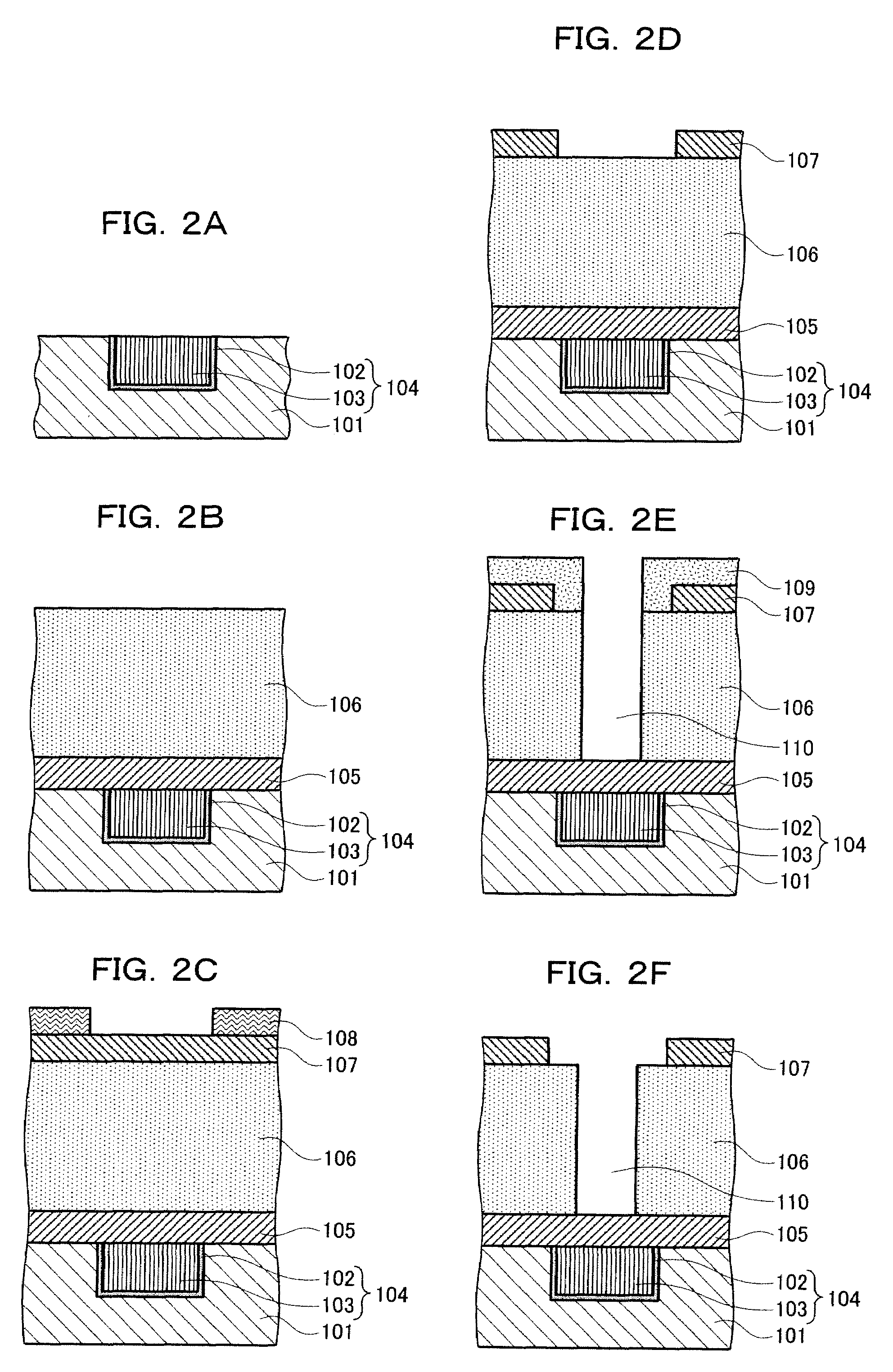
[0069]FIG. 1 is a sectional view showing the wiring structure of the semiconductor device according to the present invention. FIGS. 2A, 2B, 2C, 2D, 2E, 2F, 3A, 3B, 3C, 3D, 3E, and 3F are sectional views showing the steps of the method of manufacturing the semiconductor device according to the first embodiment of the present invention. FIG. 4 is a diagram illustrating the characteristics of the wiring resistance of the wiring structure formed according to the present invention. FIG. 5 is a diagram comparably illustrating the relationship between electric field strength and inter-wire leakage current.

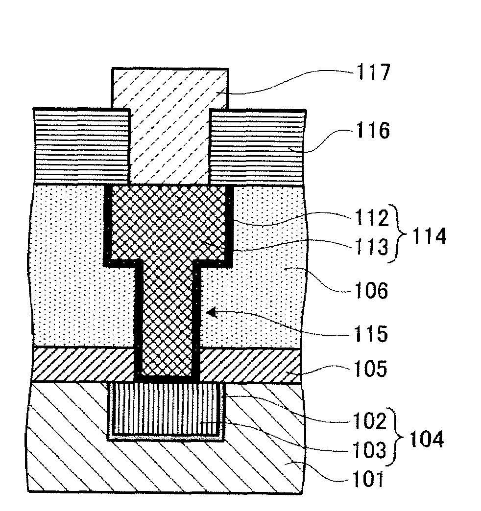
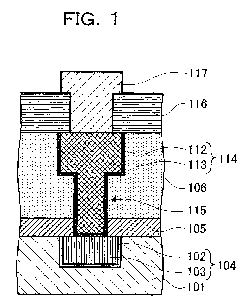
[0070]FIG. 1 shows a cross section of the wiring structure of the semiconductor device using an SiOC film as an inter-wire insulating film. In FIG. 1, a first insulating film 101 made up of the SiOC film is formed on a substrate (not shown) made up of silicon. A first metal wire 104 is formed...

second embodiment

[0087]The method of manufacturing the semiconductor device will be described with reference to FIGS. 9A, 9B, 9C, 9D, 10A,10B, 10C, and 10D.

[0088]FIGS. 9A, 9B, 9C, 9D, 10A, 10B, 10C, and 10D are sectional views showing the steps of the method of manufacturing the semiconductor device according to the second embodiment of the present invention.

[0089]The steps from the beginning of the method through the formation of the via hole of the present method are the same as the manufacturing method described in the first embodiment, shown in FIGS. 2A, 2B, 2C, 2D, 2E, and 2F. The description of these steps is thus omitted. After the via hole is formed as shown in FIG. 2F, the wiring groove 111 is formed in the third interlayer insulating film 106 by dry etching in accordance with the pattern formed on the metal hard mask 107 as shown in FIG. 9A. Then, as shown in FIG. 9B, a burial material 118 made up of an organic material is applied into the opening using a spin-coating method. Then, as sho...


PUM


Abstract

In a method of manufacturing a semiconductor device which method is made up of a process of forming a wiring groove using a hard mask, a metal hard mask 107 is used to form a wiring groove 111, allowing the shape of the wiring groove 111 to be stabilized. Furthermore, a part or all of the metal hard mask 107 is removed before the formation of TaN and Cu layers in the wiring groove 111. This enables a reduction in possible damage, which may increase the dielectric constant of the surface of low-dielectric-constant film, and thus in possible inter-wire leakage current. As a result, a reliable semiconductor device can be provided.

Description

FIELD OF THE INVENTION[0001]The present invention relates to a method of manufacturing a semiconductor device having a damascene structure.BACKGROUND OF THE INVENTION[0002]With the reduced size of a wiring structure and the increased number of layers in the wiring structure, much effort has recently been made to further integrate a semiconductor integrated circuit. As a method of forming a dense wiring pattern or a multilayer wiring structure, a damascene process is commonly used which forms wiring by using Cu as a wiring material and flattening the wiring material by means of CMP (Chemical Mechanical Polishing). On the other hand, the denser wiring pattern has disadvantageously increased a parasitic capacitance generated between wires. The increased parasitic capacitance reduces a speed at which signals are transmitted through the wiring. Thus, for the semiconductor integrated circuit which requires high-speed operations, it is important to reduce the parasitic capacitance between ...

Claims


Application Information

Patent Timeline
Patent Type & Authority Patents(United States)
IPC IPC(8): H01L21/44
CPCH01L21/76808H01L21/76811
Inventor TSUTSUE, MAKOTO
Owner PANASONIC SEMICON SOLUTIONS CO LTD
Why Eureka
Try Eureka