High voltage comparator using sliding input low voltage devices

a low voltage comparator and input voltage technology, applied in pulse manipulation, pulse technique, instruments, etc., can solve the problem that low voltage devices cannot sustain a voltage thereacross, and achieve the effect of reducing the number of input voltages, preventing changes in magnitude, and effectively sliding or translating

Inactive Publication Date: 2009-05-05
INTERSIL INC
View PDF4 Cites 3 Cited by
  • Summary
  • Abstract
  • Description
  • Claims
  • Application Information

AI Technical Summary

Benefits of technology

[0008]The high voltage devices, on the other hand, can sustain relatively high voltages, so that they can accommodate a relatively wide range of potential variation of the input voltage. These devices are used to provide high input protective buffering for the low voltage devices, and are connected in a circuit configuration with the low voltage devices that causes operating levels of the low voltage devices to move up and down or ‘slide’ with a variation in the input voltage, and thereby prevents application of a voltage thereacross greater than the relatively small range of variation that can be sustained by the low voltage devices.
[0019]However, because the differential amplifier transistor is connected in emitter-follower configuration to the emitter-follower transistor, the voltage at the base of the differential amplifier transistor is one Vbe below the voltage at the base of the emitter-follower transistor. As a result, the mutually opposing Vbe's through the level-shift and emitter-follower transistors sum to zero, so that there is a net voltage drop of zero across the base and collector of the differential amplifier transistor. Thus, there is no effective voltage differential across any of the low voltage transistors, since the circuit architecture of the comparator causes the voltages across these transistors to effectively ‘slide’ or translate with the input voltage, and thereby prevents changes in the magnitude of the input voltage from producing a (potential damaging) differential voltage across these devices.
[0020]As noted above, the current outputs of the upper and lower comparator input stages are mirrored by associated output current mirror circuits and then summed at the input resistor of a transimpedance amplifier stage. The transimpedance amplifier stage is comprised of an inverter with a resistor connected between its input and output that produces an amplified output representative of the voltage differential across the comparator's inputs, in accordance with the summation of the mirrored currents supplied to the summing input node. The combination of summed current mirror outputs and high gain transimpedance amplifier circuitry enables a small swing in the output of the differential amplifiers of the comparator's upper and lower input stages to provide large output voltage and current drive capability over the full range of variation of the input voltage.

Problems solved by technology

The low voltage devices cannot sustain a voltage thereacross that is greater than a relatively small range of variation (e.g., on the order of one to only a few volts).

Method used


Image

  • High voltage comparator using sliding input low voltage devices
  • High voltage comparator using sliding input low voltage devices
  • High voltage comparator using sliding input low voltage devices

Examples


Embodiment Construction

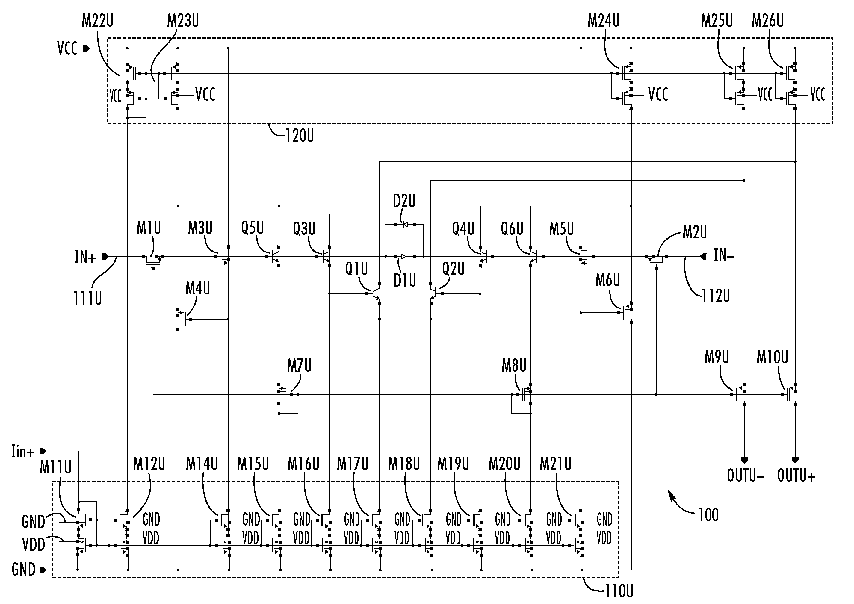
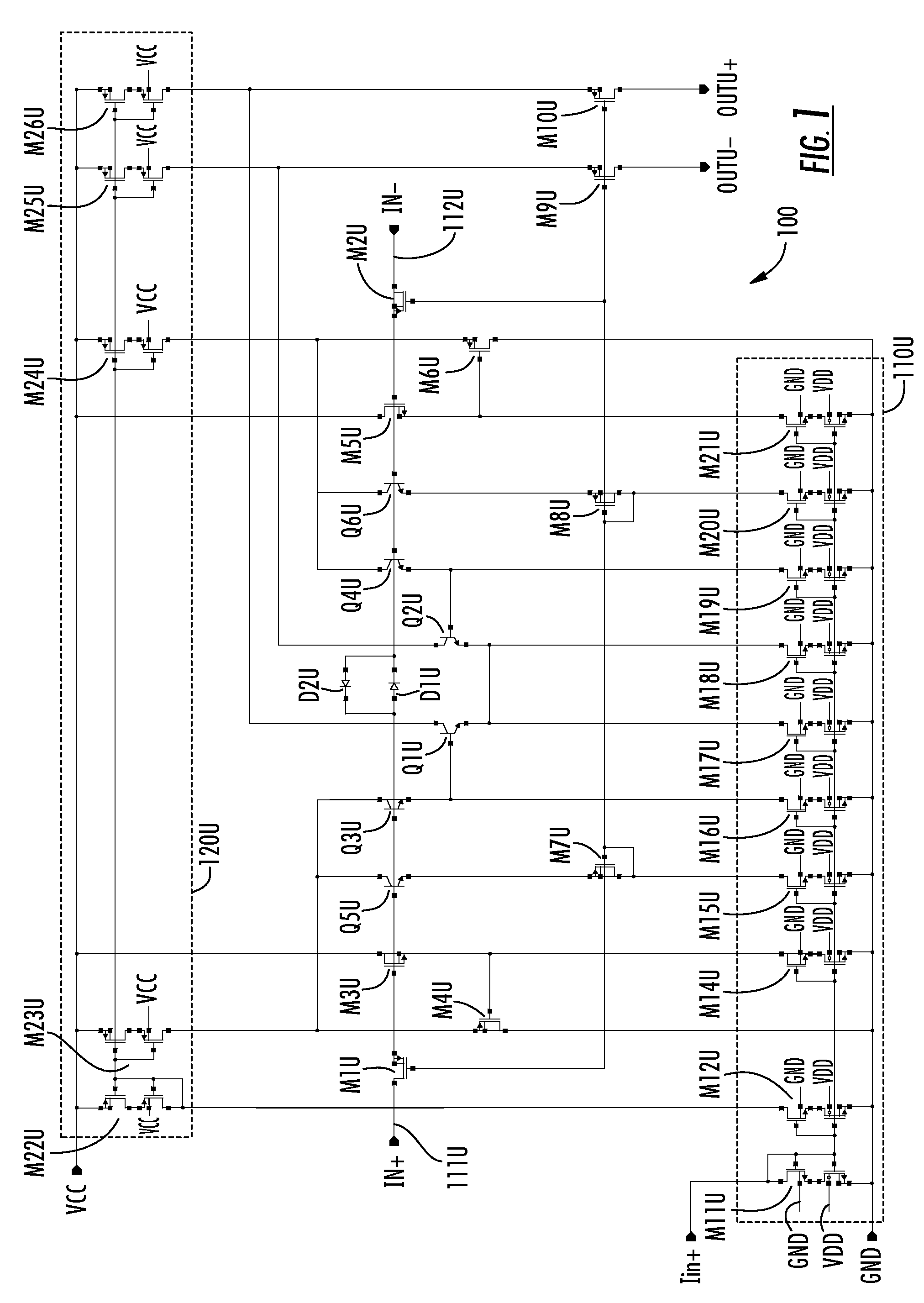
[0024]Attention is initially directed to FIG. 1, wherein a first, or upper (U) high voltage level-processing input stage 100 of the comparator circuit architecture in accordance with present invention is schematically illustrated. As pointed out briefly above, this upper comparator input stage is operative to handle input voltages (applied to differential inputs IN+ and IN−) whose amplitudes are relatively close to, or in the neighborhood of, the relatively large magnitude supply voltage of the upper power supply rail (Vcc—which may be on the order of three to twenty-eight volts, as a non-limiting example). In particular, upper comparator input stage 100 is operative to handle an input voltage lying in a range of from (Vdsat+Vgs+Vbe) to (Vcc−Vdsat), where Vdsat is the drain-source voltage for the saturated condition of an MOS transistor, Vgs is the MOS transistor gate-source voltage, and Vbe is the base-emitter voltage of a bipolar transistor.

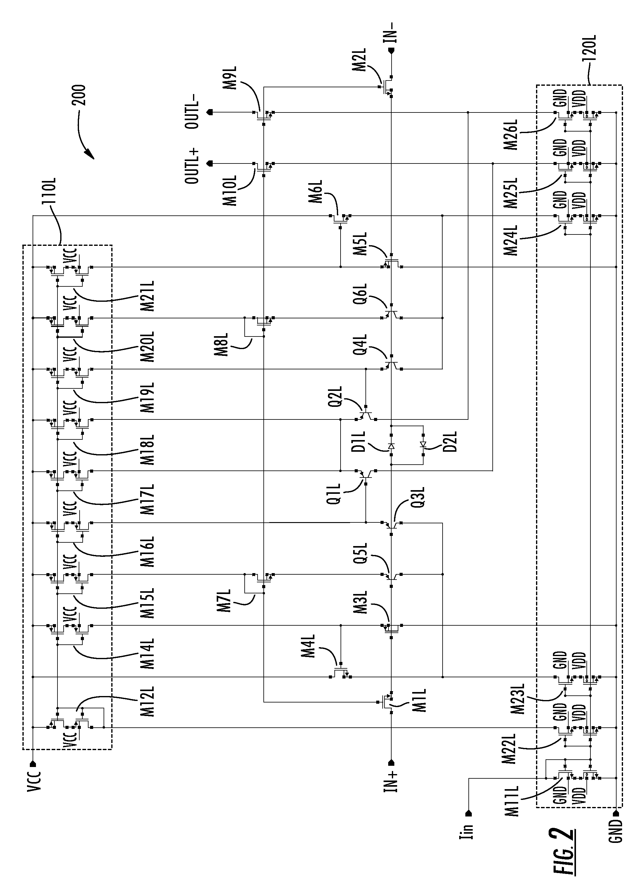
[0025]Connected in parallel with the upp...


PUM


Abstract

A voltage comparator contains low voltage devices (e.g., bipolar or MOS transistors) and high voltage devices (e.g., DMOS transistors). The low voltage devices, which cannot sustain a voltage greater than a relatively small range of variation that is substantially less than the range of potential variation of the input voltage, are connected in a differential amplifier configuration to perform precision differential measurements on the input voltage. The high voltage devices are interconnected with the low voltage devices in a manner that enables operating levels of the low voltage devices to move up / down, or ‘slide’, with variations in the input voltage, so that the low voltage devices are effectively immune to high levels of the input voltage.

Description

FIELD OF THE INVENTION[0001]The present invention relates in general to DC power supply systems and subsystems thereof, and is particularly directed to a new and improved voltage comparator circuit architecture, such as may be employed as an over-current detection comparator for a pulse width modulation (PWM) controller of a DC-DC converter, which employs low voltage devices for performing precision differential measurements on input voltages whose magnitudes may be considerably larger than voltages that can be sustained by such low voltage devices. The low voltage devices are connected with high voltage devices so as to provide high input protective buffering for the low voltage devices, and enable the operating levels of the low voltage devices to move up and down or ‘slide’ with variations in the magnitude of the input voltage being monitored.BACKGROUND OF THE INVENTION[0002]DC-DC converters are commonly used to supply DC power to a variety of electronic systems and devices, such...

Claims


Application Information

Patent Timeline
Patent Type & Authority Patents(United States)
IPC IPC(8): H03F3/45
CPCH03K5/2481
Inventor CAN, SUMER
Owner INTERSIL INC
Why Eureka
Try Eureka