

Method of manufacturing a dielectric layer and corresponding semiconductor device
a manufacturing method and semiconductor technology, applied in the direction of semiconductor/solid-state device details, fixed capacitors, coatings, etc., to achieve the effect of accelerating the reaction of the second material
- Summary
- Abstract
- Description
- Claims
- Application Information
AI Technical Summary
Benefits of technology
Problems solved by technology
Method used
Image

Examples
Embodiment Construction
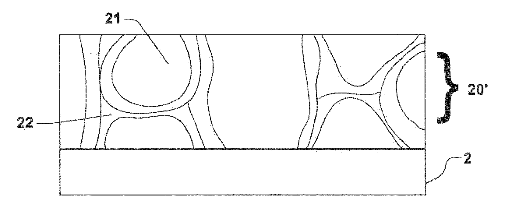
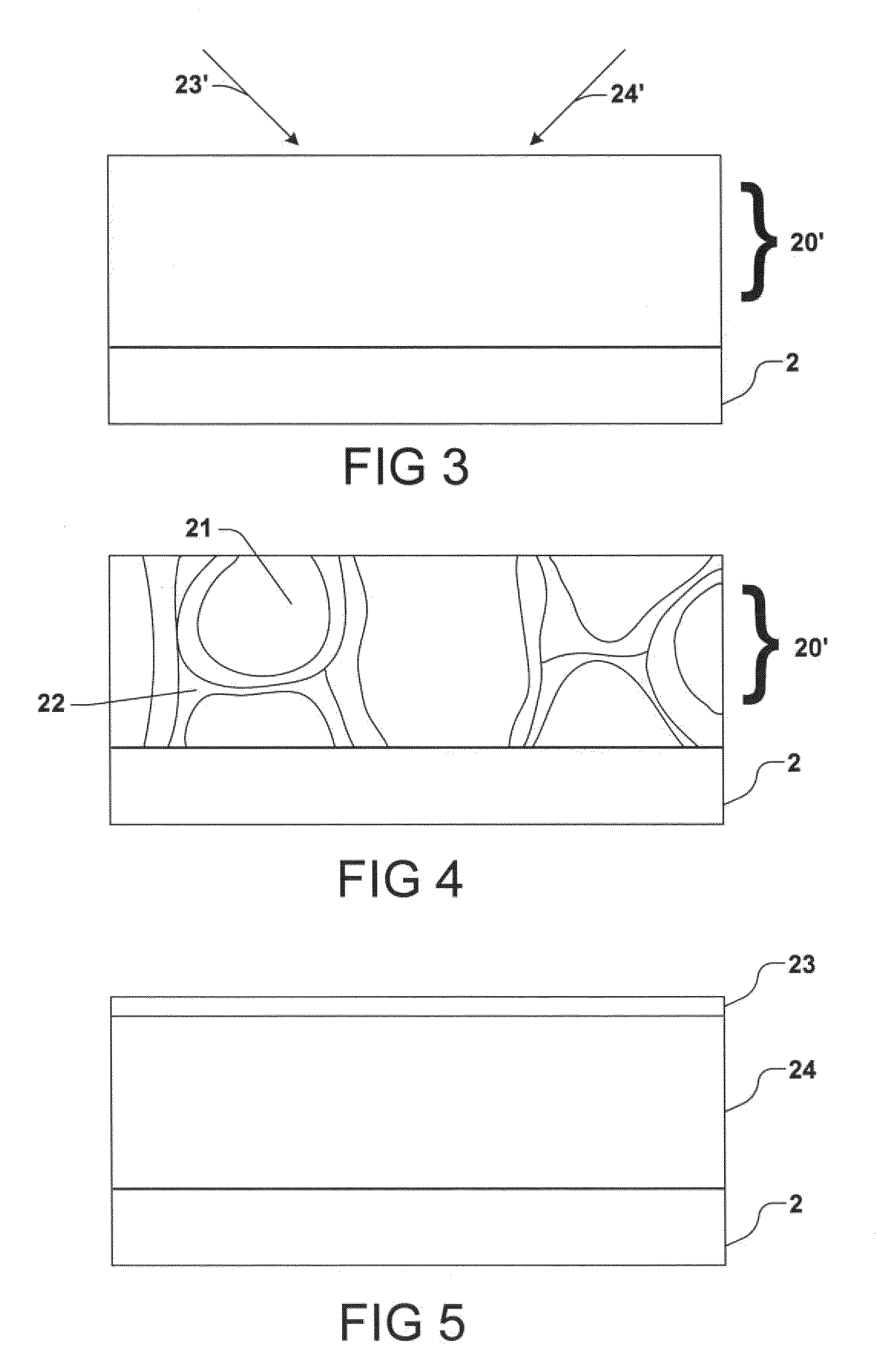
[0021]FIG. 3 illustrates a process step of a preferred embodiment of the present invention. A substrate 2 is provided. A dielectric layer 20′ is deposited via an ALD 20 (Atomic Layer Deposition) process. A first dielectric material 24′ may be deposited with a one or two precursors. The first dielectric material is selected from a group of materials having a high permittivity (high-k dielectrics). This material may be magnesium oxide, aluminium oxide, titan oxide, tungsten oxide, tantalum oxide or other oxides chosen for high-k dielectrics. Along with the deposition of the first dielectric material 24′, a second material 23′ may be introduced into the same reaction chamber in small amounts such that its contribution to the dielectric layer 20′ remains below 1% in weight. The second material may be transported as well by a precursor, as indicated in FIG. 3 by the flash, or simply added to the atmosphere in the reaction chamber.
[0022]After the deposition of the dielectric layer 20, hig...
PUM
| Property | Measurement | Unit |
|---|---|---|
| thickness | aaaaa | aaaaa |
| thickness | aaaaa | aaaaa |
| width | aaaaa | aaaaa |
Abstract
Description
Claims
Application Information