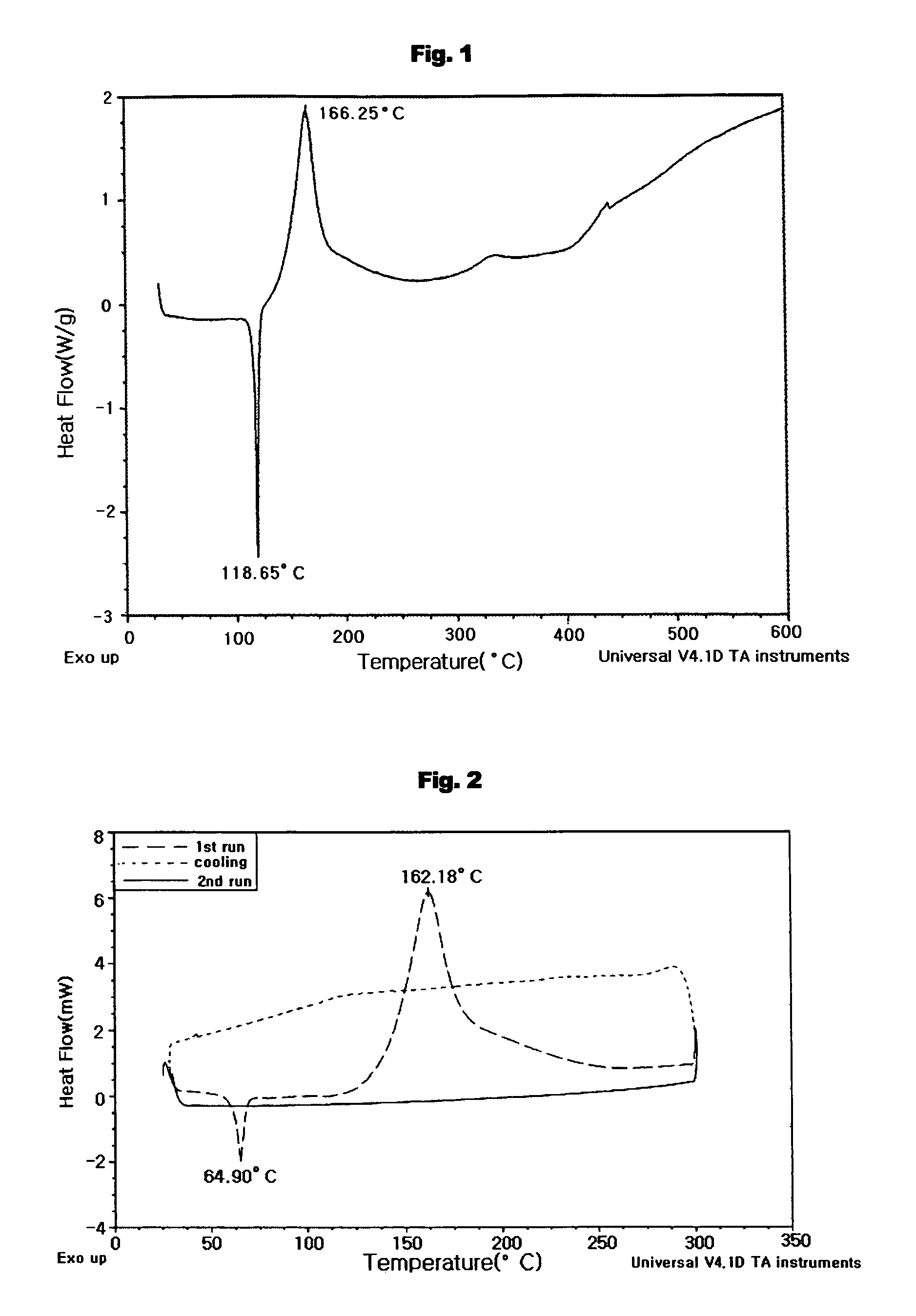
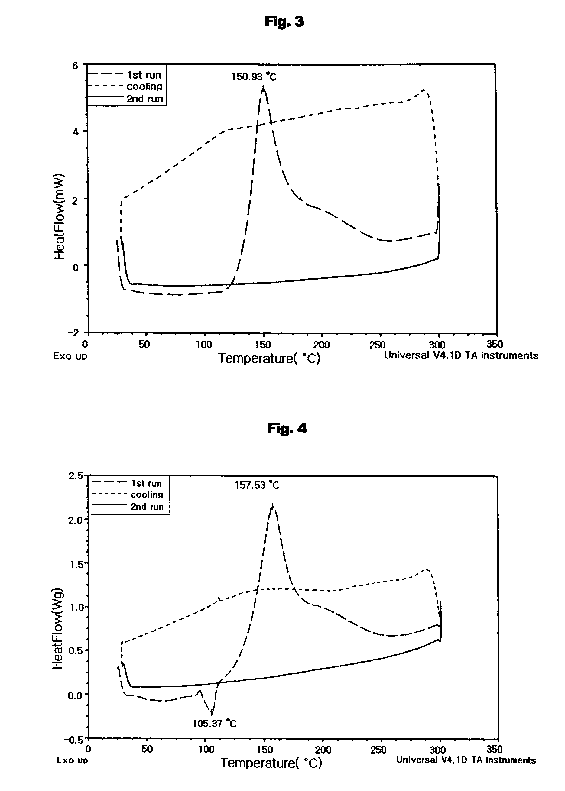
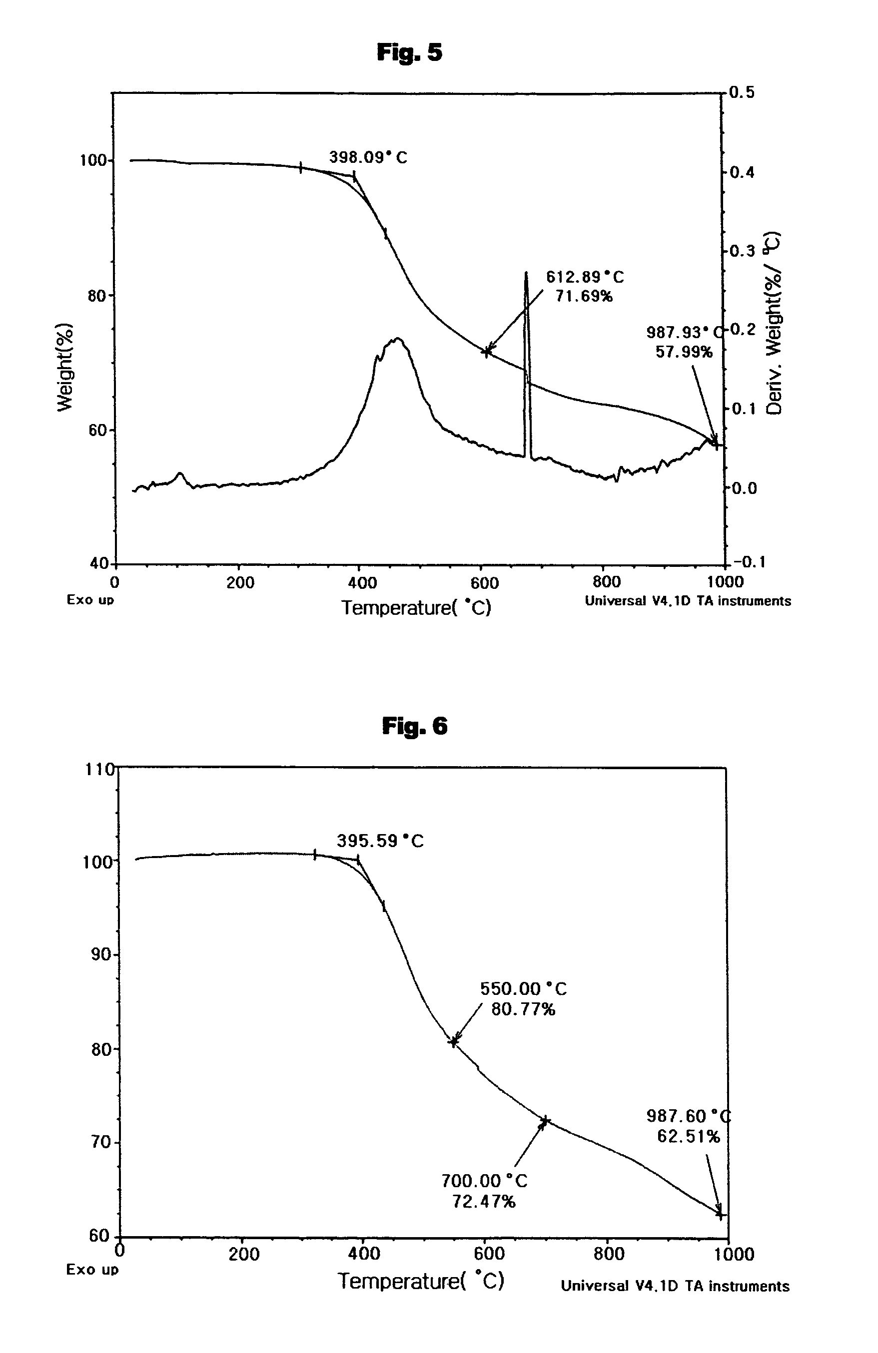
Aromatic enediyne derivatives, organic semiconductor thin films using the same and manufacturing methods thereof, and electronic devices incorporating such films

a technology of organic semiconductor and eniyne, which is applied in the field of aromatic eniyne derivatives, organic semiconductor thin films, and manufacturing methods thereof, can solve the problems of difficulty in forming a generally uniform layer across large areas of substrates, known deficiencies, and expense associated with forming layers of such materials, so as to improve chemical and/or electrical stability, the effect of improving functionality and/or reliability

Inactive Publication Date: 2009-05-19
SAMSUNG ELECTRONICS CO LTD
View PDF2 Cites 1 Cited by
  • Summary
  • Abstract
  • Description
  • Claims
  • Application Information

AI Technical Summary

Problems solved by technology

These materials, however, are known to have deficiencies including, for example, the expense associated with forming layers of such materials and difficulty forming a generally uniform layer across large areas of a substrate.
These deficiencies are, to some degree, attributable to the need to use expensive vacuum deposition apparatus in forming thin films from these lower molecular weight organic materials and an associated difficulty in forming fine patterns.
However, such organic semiconductors may be chemically unstable during the subsequent processing necessary to complete the fabrication of a semiconductor device and are accordingly difficult to implement in an actual device manufacturing line.
Moreover, results obtained by repeated current-electron sweeping for evaluating electrical stability tends to exhibit a lack of electrical stability that may result in both reduced gate threshold voltage, increased leakage currents and / or reduced reliability of the resulting devices.
However, the organic compounds and the methods of manufacturing thin films from such organic compounds may require a vacuum deposition process in order to manufacture a thin film.
Accordingly, the use of lower molecular weight compounds, for example, pentacene, may be expensive and generally unsuited for preparing organic semiconductor films over a large substrate area for cost-sensitive products.

Method used


Image

  • Aromatic enediyne derivatives, organic semiconductor thin films using the same and manufacturing methods thereof, and electronic devices incorporating such films
  • Aromatic enediyne derivatives, organic semiconductor thin films using the same and manufacturing methods thereof, and electronic devices incorporating such films
  • Aromatic enediyne derivatives, organic semiconductor thin films using the same and manufacturing methods thereof, and electronic devices incorporating such films

Examples


example 2

PREPARATIVE EXAMPLE 2

Synthesis of Example Aromatic Enediyne Derivative B

[0072]

[0073]0.25 g (1 mmol) of 2,2′:5′,2″-terthiophene, commercially available from Aldrich under the Product No. 31, 107-3, was added to chloroform, and 0.35 g (2.0 mmol) of N-bromosuccinimide was added thereto, thus obtaining dibromide 1b, which was then subjected to Suzuki coupling and desilylation under the same synthetic conditions as in the synthesis of the derivative A, thereby yielding the derivative B. Analysis of the derivative B produced the following NMR data: 1H NMR (300 MHz, CDCl3), δ(ppm) 0.93 (t, 6H, J=7.2 Hz), 1.24-1.67 (m, 12H), 2.51 (t, 4H, J=7.0 Hz), 3.26 (s, 2H), 7.05-7.08 (m, 8H).

example 3

PREPARATIVE EXAMPLE 3

Synthesis of Example Aromatic Enediyne Derivative C

[0074]

[0075]5,5′-dibromo-2,2′-bithiophene, commercially available from Aldrich under the Product No. 51.549-3, and 2-thiopheneboronic acid, commercially available from Aldrich under the Product No. 43, 683-6, were subjected to Suzuki coupling, thus obtaining a predetermined or desired product, which was then added with N-bromosuccinimide to prepare dibromotetrathiophene 1c. Subsequently, the compound 1c was subjected to Suzuki coupling and desilylation under the same synthetic conditions as in the synthesis of the derivative A, therefore yielding the derivative C. Analysis of the derivative C produced the following NMR data: 1H NMR (300 MHz, CDCl3), δ(ppm) 0.93 (t, 6H, J=7.2 Hz), 1.24-1.67 (m, 12H), 2.51 (t, 4H, J=7.0 Hz), 3.27 (s, 2H), 7.05-7.09 (m, 10H).

example 4

PREPARATIVE EXAMPLE 4

Synthesis of Example Aromatic Enediyne Derivative D

[0076]

[0077]1 g (4.2 mmol) of 1,4-dibromobenzene, commercially available from Aldrich under the Product No. D3,902-9, was subjected to Suzuki coupling with 2-bromothiophene, to prepare 0.72 g (3.0 mmol) of a predetermined or desired product, which was then added to chloroform, and 1.1 g (6.2 mmol) of N-bromosuccinimide was added thereto, thus preparing 0.6 g of dibromide 1d. Subsequently, the compound 1d was subjected to Suzuki coupling and desilylation under the same synthetic conditions as in the synthesis of the derivative A, therefore yielding the derivative D. Analysis of the derivative D produced the following NMR data: 1H NMR (300 MHz, CDCl3), δ(ppm) 0.93 (t, 6H, J=7.2 Hz), 1.24-1.67 (m, 12H), 2.51 (t, 4H, J=7.0 Hz), 3.27 (s, 2H), 7.01 (s, 2H), 7.13 (d, 2H, J=3.8 Hz), 7.25 (d, 2H, J=3.8 Hz), 7.60 (s, 4H).


PUM

PropertyMeasurementUnit
temperatureaaaaaaaaaa

Abstract

Disclosed are aromatic enediyne derivatives, methods of manufacturing organic semiconductor thin films from such aromatic enediyne derivatives, and methods of fabricating electronic devices incorporating such organic semiconductor thin films. Aromatic enediyne derivatives according to example embodiments provide improved chemical and / or electrical stability which may improve the reliability of the resulting semiconductor devices. Aromatic enediyne derivatives according to example embodiments may also be suitable for deposition on various substrates via solution-based processes, for example, spin coating, at temperatures at or near room temperature to form a coating film that is then heated to form an organic semiconductor thin film. The availability of this reduced temperature processing allows the use of the aromatic enediynes derivatives on large substrate surfaces and / or on substrates not suitable for higher temperature processing. Accordingly, the organic semiconductor thin films according to example embodiments may be incorporated in thin film transistors, electroluminescent devices, solar cells, and memory devices.

Description

BACKGROUND[0001]1. Technical Field[0002]Example embodiments relate to aromatic enediyne derivatives, organic semiconductor thin films formed using such aromatic enediyne derivatives and methods of manufacturing such films, and electronic devices incorporating such organic semiconductor thin films and methods of manufacturing such devices, and, for example, to organic semiconductor thin films fabricated from such aromatic enediyne derivatives that exhibit improved chemical and electrical stability. The aromatic enediyne derivatives according to example embodiments may be applied to substrates via solution-based processes, for example, spin coating, and are suitable for application at or near room temperature to form a coating layer that, after thermal treatment, may form an organic semiconductor thin film on the substrate that may be used in forming a carrier transport layer in an electronic device incorporating such an organic semiconductor thin film.[0003]2. Description of the Rela...

Claims


Application Information

Patent Timeline
Patent Type & Authority Patents(United States)
IPC IPC(8): C07D409/14
CPCC07D333/18H01L51/0068H01L51/0545H01L51/0003Y02E10/549Y02P70/50H10K71/12H10K85/655H10K10/466
Inventor JEONG, EUN JEONGMOON, HYUN SIKHAN, KOOK MIN
Owner SAMSUNG ELECTRONICS CO LTD
Why Eureka
Try Eureka