Method and apparatus for depositing thin films on a surface

Active Publication Date: 2009-05-26
ASM IP HLDG BV
View PDF88 Cites 27 Cited by
  • Summary
  • Abstract
  • Description
  • Claims
  • Application Information

AI Technical Summary

Benefits of technology

[0016]In one embodiment, gases are exhausted through the elongated tube in route from the substrate to the outlet. Both reactant and purge gas is allowed to diffuse across gaps between the apertures and thereby saturate the substrate in each step. Advantageously, the purge steps can include multiple sequential pulses causing pressure fluctuation, which expedite diffusion between gaps in the apertures, and especially diffusion into deep narrow trenches of the substrate. Similarly, the reactant steps can include multiple sequential pulses causing pressure fluctuations to aid in diffusing reactant across the substrate or into deep, narrow features on the substrate. In one particular arrangement, a booster purge pulse, immediately prior to a standard purge pulse, helps clear reactant from the prior pulse and creates a pressure gradient, while also clearing an inert gas diffusion barrier created by an inert gas valving arrangement.

Problems solved by technology

Cycles can also be more complex.
However, only a few precursors exhibit such ideal or near ideal behavior.
However, in such a configuration, in the course of time the reacted gases may form a film in the apertures and the apertures may become blocked.
Such blockage may result in uneven deposit of layers onto the substrate.
In addition to issues with respect to blockage of the apertures, the disclosed structure contemplates relative rotation of either the substrate or the tubes during deposition.
Such a construction leads to the additional issue that, for most efficient saturation of the substrate with reactant, rotation must be calculated to be an integral value in each reactant pulse, limiting flexibility in recipe design and risking non-uniformity.
Furthermore, the complexity of rotating elements leads to risks of reactant leakage between rotating parts, consequent particle generation and / or safety hazards.

Method used


Image

  • Method and apparatus for depositing thin films on a surface
  • Method and apparatus for depositing thin films on a surface
  • Method and apparatus for depositing thin films on a surface

Examples


Embodiment Construction

[0037]While not separately illustrated, the skilled artisan will readily appreciate that the flow sequences described herein can be controlled by software programming or hardwiring arranged to open and close gas control valves in the desired sequence.

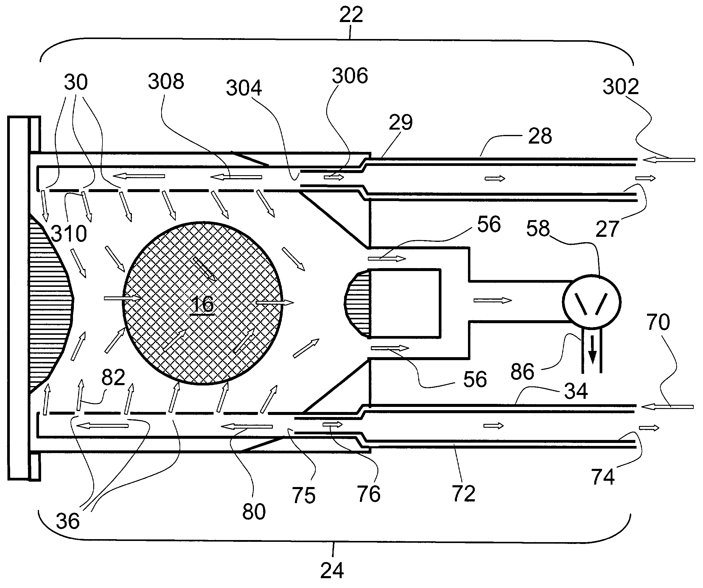
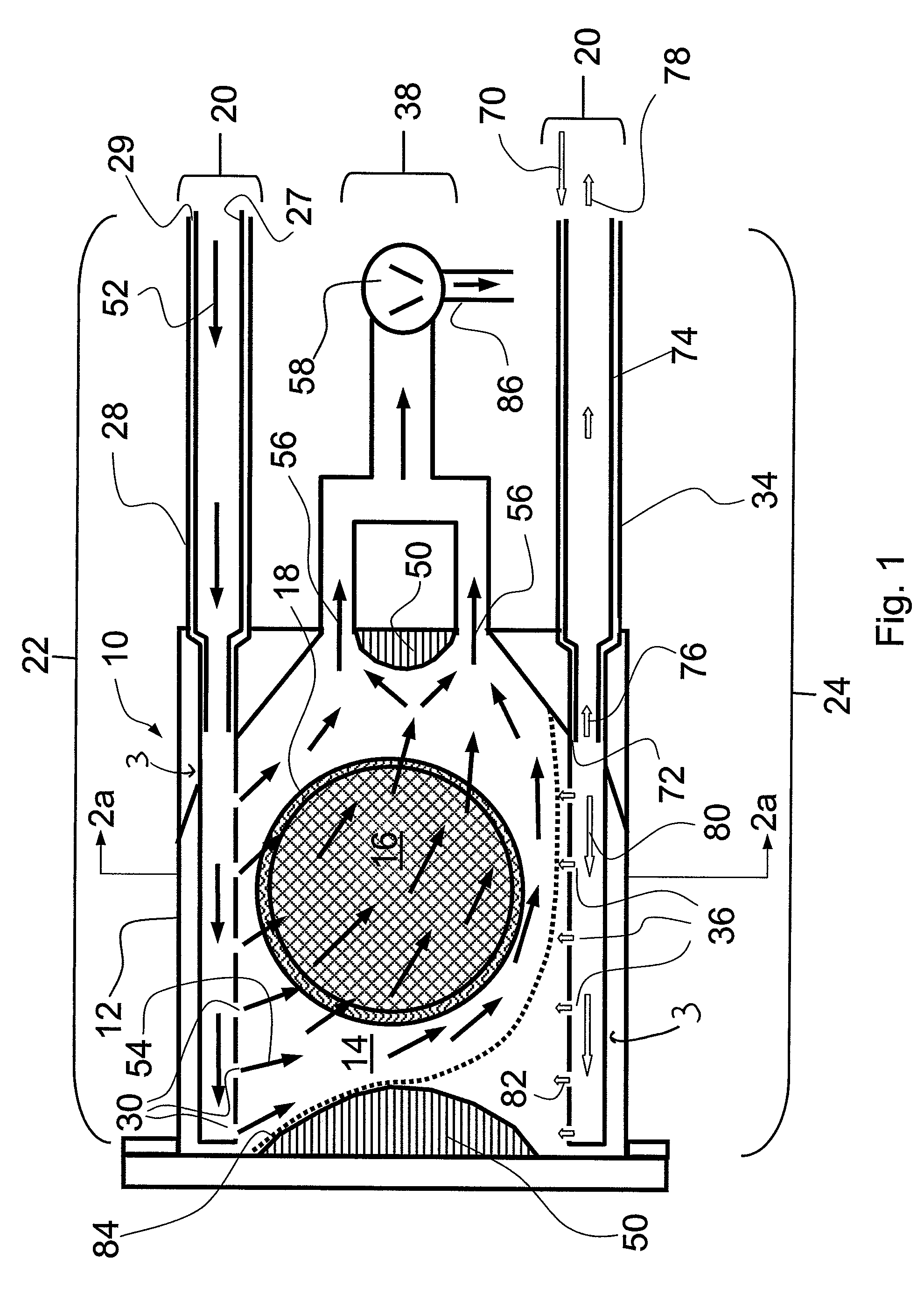
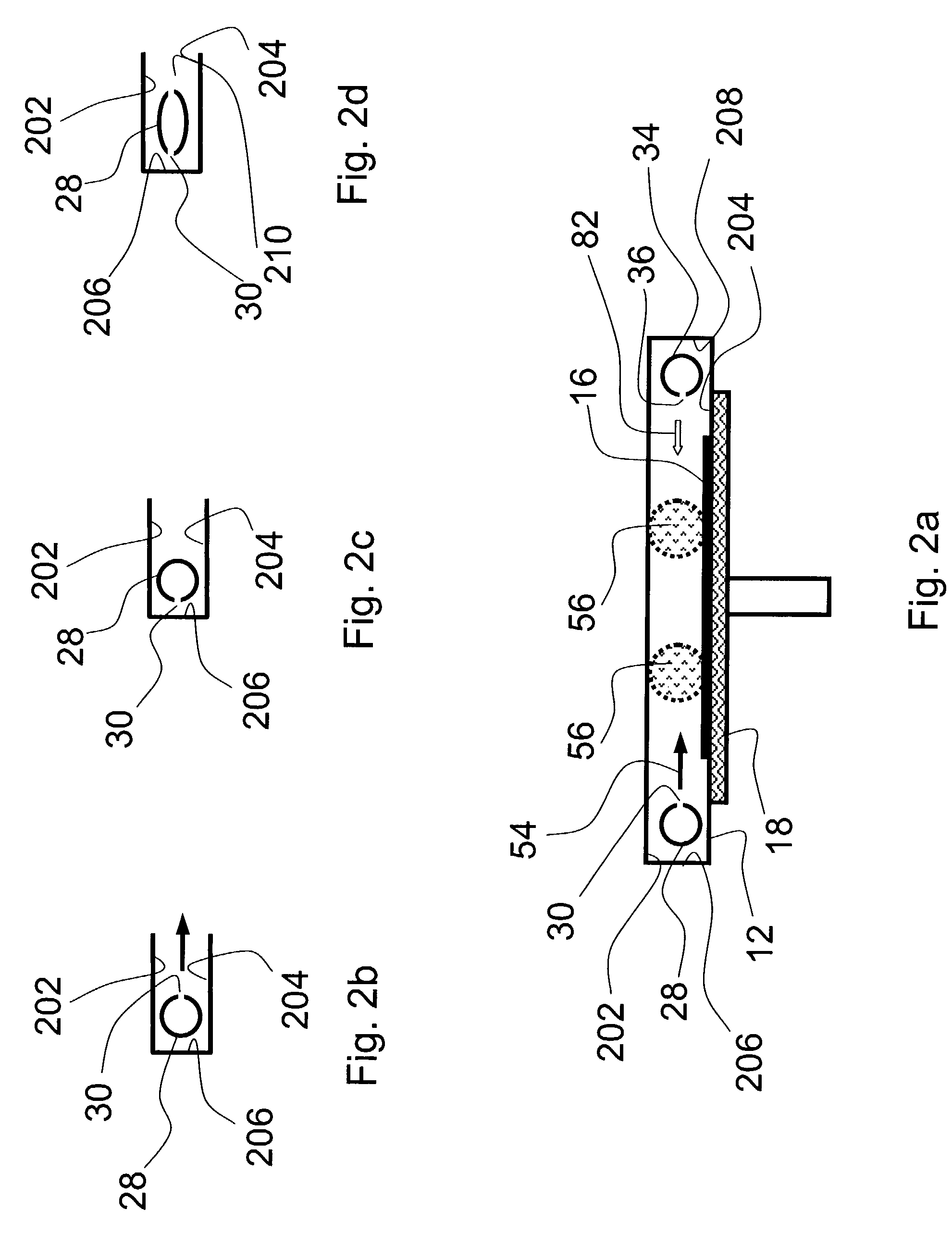
[0038]FIG. 1 illustrates a schematic top view of an embodiment of an atomic layer deposition (ALD) reactor 10. The ALD reactor 10 includes a reaction chamber 12, which defines, in part, a reaction space 14. A wafer or substrate 16 is disposed within the reaction chamber 12 and is supported by a platform or a single-substrate support. The substrate support of the illustrated embodiment also serves as a wafer handler 18 configured to move the wafer 16 in and out of the reaction chamber 12. The wafer handler 18 can be configured to receive the wafer 16 in such a way that the wafer 16 touches the handler 18 itself. Alternatively, the wafer handler can operate on the Bernoulli principle, whereby jets of inactive gas produce a low pressure zo...


PUM

PropertyMeasurementUnit
Lengthaaaaaaaaaa
Lengthaaaaaaaaaa
Lengthaaaaaaaaaa

Abstract

A method and apparatus for depositing thin films onto a substrate is provided. The apparatus includes a gas injection structure that is positioned within a reaction chamber that has a platform. The gas injection structure may be positioned above or below the platform and comprises a first gas injector and a second gas injector. The first gas injector is in fluid communication with a first reactant source and a purge gas source. Similarly, the second gas injector is in fluid communication with a second reactant source and a purge gas source. The first and second injectors include hollow tubes with apertures opening to the reaction chamber. In one configuration, the tubes are in the form of interleaved branching tubes forming showerhead rakes. Methods are provided for deposition, in which multiple pulses of purge and reactant gases are provided for each purge and reactant step.

Description

FIELD OF THE INVENTION[0001]The present invention relates generally to a semiconductor processing apparatus and more particularly, a semiconductor processing apparatus for depositing thin films on a substrate surface.BACKGROUND OF THE INVENTION[0002]Thin films may be grown on the surface of substrates by several different methods. These methods include vacuum evaporation deposition, molecular beam epitaxy (MBE), different variants of chemical vapor deposition (CVD) (including low-pressure and organometallic CVD and plasma-enhanced CVD), and atomic layer epitaxy (ALE), which has been more recently referred to as atomic layer deposition (ALD) for the deposition of a variety of materials.[0003]In ALD, the sequential introduction of precursor species (e.g., a first precursor and a second precursor) to a substrate, which is located within a reaction chamber is generally employed. Typically, one of the initial steps of ALD is the adsorption of the first precursor on the active sites of th...

Claims


Application Information

Patent Timeline
IPC IPC(8): C23C16/455C23F1/00H01L21/306C23C16/52C23C16/44
CPCC23C16/4412C23C16/45544C23C16/45565C23C16/45574
Inventor SOININEN, PEKKA J.LINDFORS, SVEN
Owner ASM IP HLDG BV
Why Eureka
Try Eureka