Carbon-modulated breakdown voltage SiGe transistor for low voltage trigger ESD applications

Inactive Publication Date: 2005-04-12
GLOBALFOUNDRIES INC
View PDF14 Cites 26 Cited by
  • Summary
  • Abstract
  • Description
  • Claims
  • Application Information

AI Technical Summary

Benefits of technology

The present invention relates to providing carbon in the structure of an SiGe transistor to modulate the redistribution of dopants in the base-collector region of the transistor, thus lowering the BVCEO of the transistor. Carbon atoms placed in the base region of a SiGe transistor influence the transient enhanced diffusion (TED) of dopants in the silicon lattice in the vicinity of the base-collector region. In the base-collector region, the base region contains boron, germanium and silicon atoms. In the collector region, the dopants can be arsenic, phosphorus, and antimony, or other n-type dopants. Placing carbon in the region below the base-collector junction region causes the dopants to diffuse either toward or away from the junction area, thereby changing the BVCEO of the transistor. The BVCEO of the transistor can be further decreased by increasing the collector's doping concentration.

Problems solved by technology

As semiconductor applications extend beyond 1 GHz applications from 10 to 100 GHz, providing ESD protection and satisfying performance goals will increase in difficulty.
With transistors whose unity current gain cutoff frequency fT exceed 10 GHz, the ability to provide ESD protection without impacting performance will be a significant challenge.
These criteria can not be satisfied by many of today's ESD solutions (e.g., silicon controlled rectifiers (SCR), and MOSFET transistors) leaving diode and diode configuration elements as a key choice for RF applications.

Method used


Image

  • Carbon-modulated breakdown voltage SiGe transistor for low voltage trigger ESD applications
  • Carbon-modulated breakdown voltage SiGe transistor for low voltage trigger ESD applications
  • Carbon-modulated breakdown voltage SiGe transistor for low voltage trigger ESD applications

Examples


Embodiment Construction

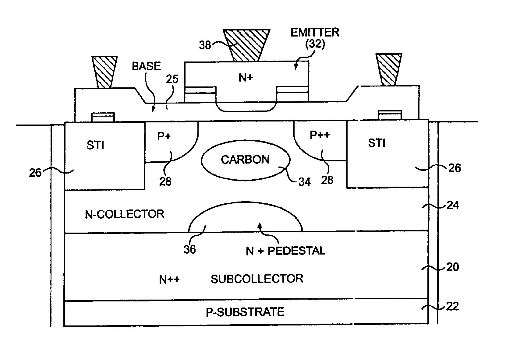
FIG. 1 shows the SiGe HBT structure for a transistor to be used in a trigger-clamp ESD protection circuit. The SiGe HBT devices are designed on a p− substrate (22). A n++ subcollector (20) is then formed over the p− substrate (22). An n− collector (24) is then formed over the n++ subcollector. The n− dopants in the n− collector (24) can be arsenic, phosphorus, and antimony, or any other type n− dopant. Shallow trench isolation areas (26) are then formed in the n− collector. The base (25) is formed by providing a ultra-high vacuum chemical vapor deposition (UHV / CVD) SiGe deposited film on the silicon surface. The extrinsic base is then formed by forming p+ (28) areas adjacent to the n− collector. An emitter (32) is then formed to overlap the p+ (28) extrinsic base areas and the n− collector (24).

A carbon implant (34) is then placed in various regions of the transistor. This carbon implant (34) promotes the migration of the n-type dopants in the collector away from the region of the p...


PUM


Abstract

Selectively implanting carbon in a transistor lowers the collector-to-emitter breakdown (BVCEO) of the transistor. This transistor, with the lowered BVCEO, is then used as a “trigger” device in an Electrostatic Discharge (ESD) power clamp comprising a first low breakdown trigger device and a second high breakdown clamp device. ESD power clamps are constructed using epitaxial base pseudomorphic Silicon Germanium heterojunction transistors in a common-collector Darlington configuration.

Description

BACKGROUND OF THE INVENTION1. Field of the InventionThe present invention relates to transistor design, and, in particular, a transistor with carbon inplants used to vary the collector-to-emitter breakdown voltage. (BVCEO).2. Background of the InventionElectrostatic discharge (ESD) protection of radio frequency (RF) products is important as application frequencies exceed 1 GHz. Below 1 GHz application frequency, the ability to simultaneously achieve excellent ESD protection and performance objectives was possible in most CMOS, BiCMOS, and SOI applications. As semiconductor applications extend beyond 1 GHz applications from 10 to 100 GHz, providing ESD protection and satisfying performance goals will increase in difficulty. Today, high speed data rate wired, wireless, test equipment and disk drive applications are extending well above 1 GHz. Today, Silicon Germanium (SiGe) technology produces heterojunction bipolar transistors that show significant increases in unity current gain cut...

Claims


Application Information

Patent Timeline
IPC IPC(8): H01L31/102H01L31/072H01L31/0264H01L31/0336H01L31/06H01L31/0328H01L31/109H01L27/02H01L29/08H01L29/24H01L29/737
CPCH01L29/7378H01L29/0821H01L27/0259H01L29/1608
Inventor COOLBAUGH, DOUGLAS D.VOLDMAN, STEVEN H.
Owner GLOBALFOUNDRIES INC
Why Eureka
Try Eureka