Substrate coupled noise isolation for integrated circuits

a technology of integrated circuits and substrates, applied in the field of reducing substrate noise coupling, can solve the problems of affecting the overall performance of noise sensitive circuits, altering their operating points,

Active Publication Date: 2009-06-02
XILINX INC
View PDF2 Cites 19 Cited by
  • Summary
  • Abstract
  • Description
  • Claims
  • Application Information

AI Technical Summary

Benefits of technology

[0010]The substrate coupled noise isolation within integrated circuit of the present invention substantially meets these needs and others. In one embodiment, an integrated circuit includes a substrate, a noise sensitive circuit, and a first low impedance guard ring. The substrate includes a well-doped blocking ring that at least partially surrounds the noise sensitive circuit. The noise sensitive circuit is fabricated on the substrate. The first low impedance guard ring is fabricated on the substrate to at least partially surround the well-doped blocking ring, wherein the first low impedance guard ring is operably coupled to a first circuit ground, wherein impedance of the first low impedance guard ring is substantially less than impedance of the well-doped blocking ring.
[0011]In another embodiment, a serializer/deserializer (SERDES) module includes a Serial-Input-Parallel-Output (SIPO) module, a Parallel-Input-Serial-Output (PISO) module, a first well-doped blocking ring, a second well-doped blocking ring, a first low impedance guard ring, and a second low impedance guard ring. The SIPO module converts inbound high-speed serial data into inbound parallel data, wherein the SIPO module includes a first noise sensitive circuit and wherein the SIPO module is fabricated on a substrate of an integrated circuit. The PISO module converts outbound parallel data into high-speed outbound serial data, wherein the PISO module includes a second noise sensitive circuit and wherein the PISO module is fabricated on the substrate of the integrated circuit. The first well-doped blocking ring is fabricated on the substrate to at least partially surround the first noise sensitive circuit. The second well-doped blocking ring is fabricated on the substrate to at least partially surround the second noise ...

Problems solved by technology

In particular, the substrate coupled noise causes the voltage of the drain and/or gate of the transistor of the noise sensitive circuit to vary, which alters its operating point.
As such, the substrate c...

Method used


Image

  • Substrate coupled noise isolation for integrated circuits
  • Substrate coupled noise isolation for integrated circuits
  • Substrate coupled noise isolation for integrated circuits

Examples


Embodiment Construction

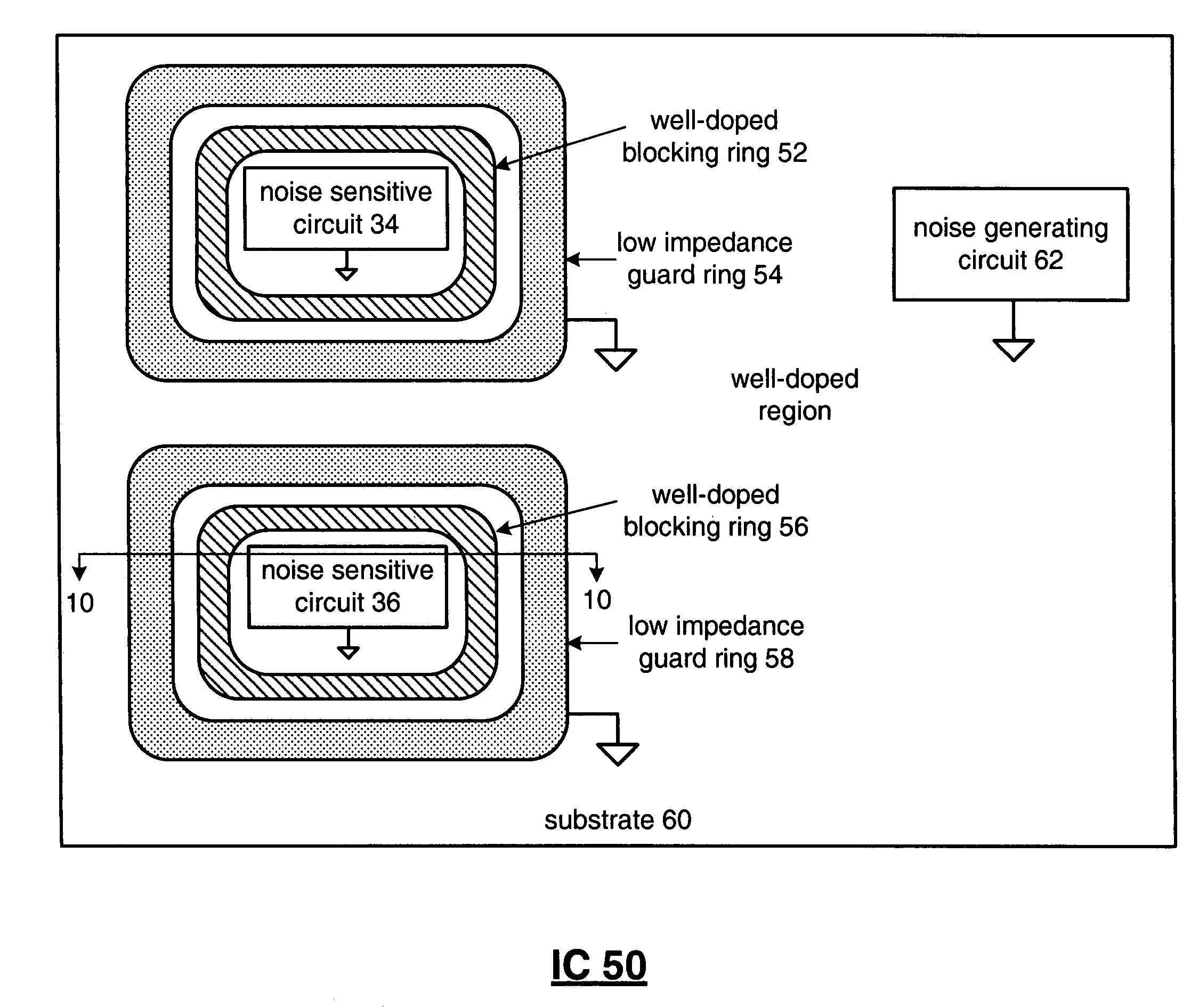
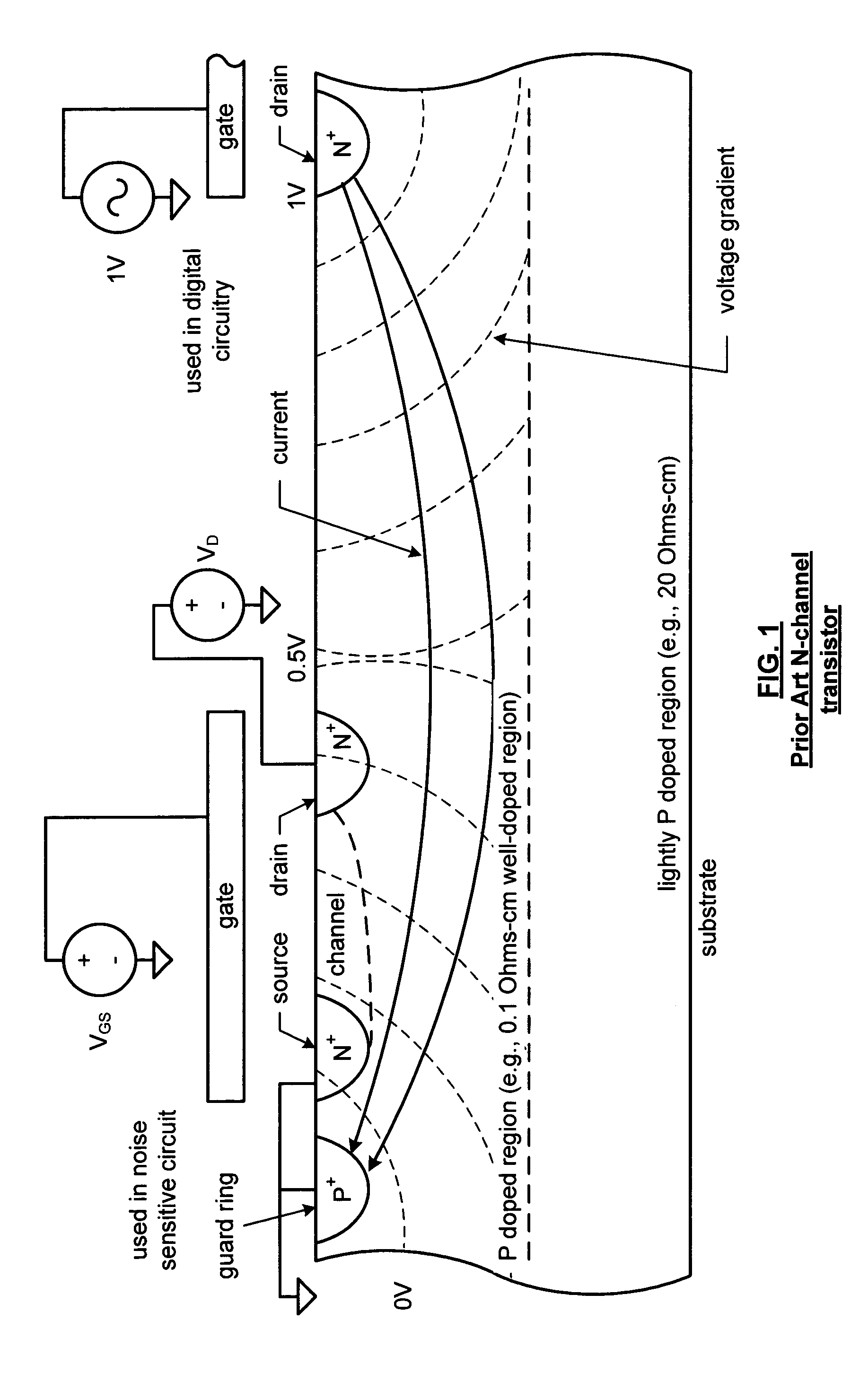
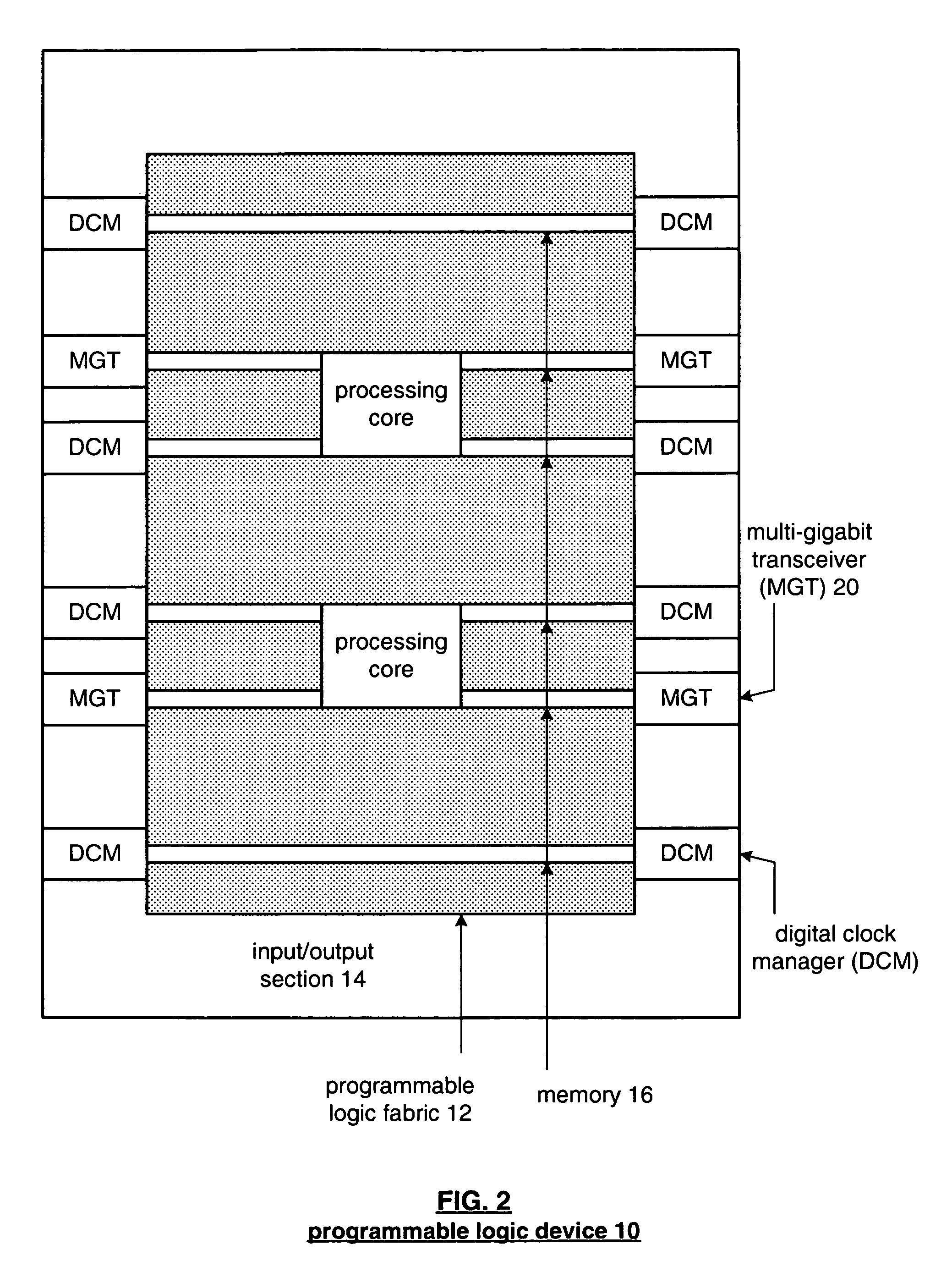
[0024]FIG. 2 is a schematic block diagram of a programmable logic device 10 that includes programmable logic fabric 12, an input / output section 14, and memory 16. The programmable logic fabric 12 may include one or more processing cores and programmable logic circuitry. Such programmable logic circuitry may include programmable logic arrays (PLAs), programmable array logic (PAL) devices, erasable programmable logic devices (EPLDs) and / or programmable gate arrays (PGAs). Memory 16 may be block random access memory (BRAM). Input / output section 14 may include a plurality of digital clock managers (DCMs) and a plurality of multi-gigabit transceivers (MGTs). An alternative embodiment of a programmable logic device may be found in U.S. patent application Ser. No. 10 / 683,944 by Young, which is incorporated herein in its entirety.

[0025]The digital clock managers provide various clock signals to the programmable logic fabric 12 and may further provide clock signals to the multi-gigabit trans...


PUM


Abstract

An integrated circuit includes a substrate, a noise sensitive circuit, and a first low impedance guard ring. The substrate includes a well-doped blocking ring that at least partially surrounds the noise sensitive circuit. The noise sensitive circuit is fabricated on the substrate. The first low impedance guard ring is fabricated on the substrate to at least partially surround the well-doped blocking ring, wherein the first low impedance guard ring is operably coupled to a first circuit ground, wherein impedance of the first low impedance guard ring is substantially less than impedance of the well-doped blocking ring.

Description

BACKGROUND OF THE INVENTION[0001]1. Technical Field of the Invention[0002]This invention relates generally to integrated circuits and more particularly to reducing substrate noise coupling.[0003]2. Description of Related Art[0004]FIG. 1 is a cross-sectional view of a prior art N-channel transistor fabricated on a substrate. As shown, the N-channel transistor includes two N-doped implants to produce a source and drain. The N-channel transistor further includes a gate and a P-doped implant that functions as a guard ring. To activate the N-channel transistor, a voltage VDS is provided to the drain and a voltage VGS is provided to the gate.[0005]In many applications, the N-channel transistor may be used in noise sensitive circuitry such as amplifiers, buffers, analog-to-digital converters, et cetera. As is often the case, an integrated circuit has millions of transistors on its substrate, some of which are used in digital circuitry that produces noise, which is coupled into the substrat...

Claims


Application Information

Patent Timeline
IPC IPC(8): H01L29/72
CPCH01L21/761H01L21/823481H01L23/585H01L29/0619H01L29/78H01L2924/3011H01L2924/0002H01L2924/00
Inventor ABUGHAZALEH, FIRAS N.
Owner XILINX INC
Why Eureka
Try Eureka