Laser light coupling into soi CMOS photonic integrated circuit

a photonic integrated circuit and laser light technology, applied in the field of optics, can solve the problems of large footprint, integrated solution, and important fiber coupling cost, and achieve the effect of less complex

Active Publication Date: 2012-12-20
UNIV GENT +1
View PDF0 Cites 97 Cited by
  • Summary
  • Abstract
  • Description
  • Claims
  • Application Information

AI Technical Summary

Benefits of technology

[0043]The method may comprise processing the first substrate to introduce further components to generate an integrated photonic circuit, thus generating an integrated photonics circuit with embedded hybrid laser. It is an advantage of embodiments of the present invention that the hybrid laser can be part of an integrated photonic circuit and that processing can be done during the same or similar processing steps.
[0044]The method furthermore may comprise packaging the integrated photonic circuit with embedded hybrid laser in a single packaging

Problems solved by technology

This has an advantage in terms of thermal isolation but is not an integrated solution and so has a larger footprint.
Furthermore, there is an important fiber coupling cost.
Tight mechanical alignment requir

Method used


Image

  • Laser light coupling into soi CMOS photonic integrated circuit
  • Laser light coupling into soi CMOS photonic integrated circuit
  • Laser light coupling into soi CMOS photonic integrated circuit

Examples


Embodiment Construction

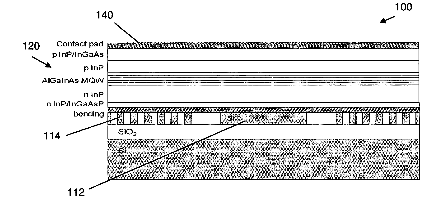
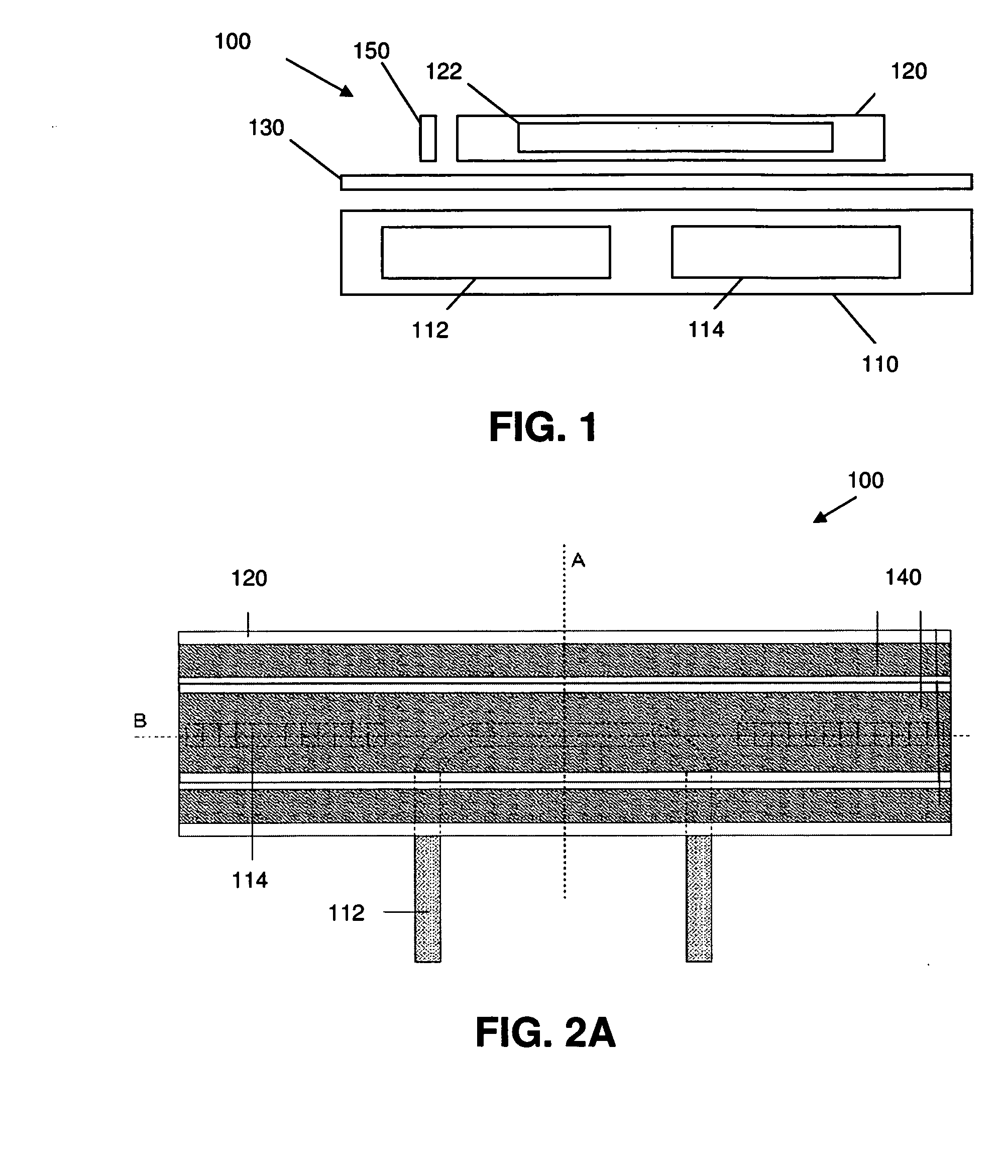
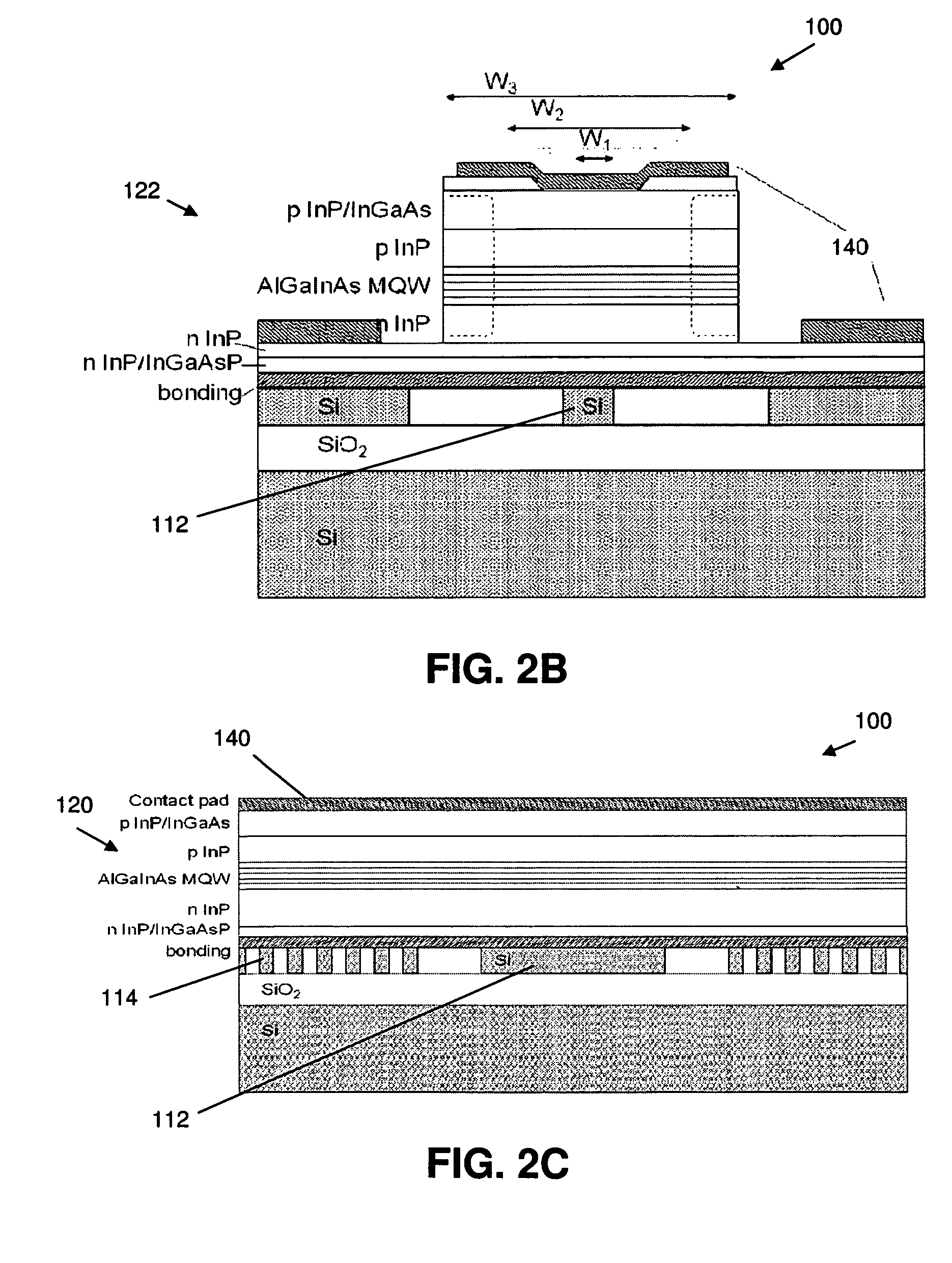
[0064]Whereas in embodiments illustrating the devices and methods of the present invention often reference is made to a silicon on insulator (SOI) material system in combination with a III-V optical active material, embodiments of the present invention are not limited thereto and relate to use of a high index contrast optical passive material, such as for example an SOI material system, silicon, germanium, silicon germanium, silicon nitride, silicon carbide, etc. in combination with use of an optical active material, e.g. an optical active semiconductor material. The optical passive material and optical active material may be single materials or a combination of materials, such as for example a stack of materials. Silicon-on-Insulator, nevertheless is a very interesting material system for highly integrated photonic circuits. The high refractive index contrast allows photonic waveguides and waveguide components with submicron dimensions to guide, bend and control light on a very sma...


PUM


Abstract

A hybrid laser for generating radiation includes an optical passive material and an optical active material. The laser includes a first optical waveguide and optical laser components with reflectors in the optical passive material. The first optical waveguide is adapted for coupling out radiation from the hybrid laser. The laser also includes a second optical waveguide defined in the optical active material. The optical laser components include reflectors defining a cavity and furthermore are adapted for providing laser cavity confinement in the first optical waveguide and the second optical waveguide. The second optical waveguide thereby is positioned at least partly over the first optical waveguide so that an evanescent coupling interface is defined between the second optical waveguide and the first optical waveguide and the evanescent coupling interface is positioned within the laser cavity.

Description

FIELD OF THE INVENTION[0001]The invention relates to the field of optics. More particularly, the present invention relates to hybrid laser systems and corresponding methods for generating laser radiation.BACKGROUND OF THE INVENTION[0002]Silicon photonics has gained increased attention in recent years because of its potential to significantly reduce the cost of optical devices used in traditional applications and its potential to enable new applications. Silicon Photonic Integrated Circuits (PICs) can be fabricated using standard, wafer scale CMOS technology, allowing a drastic reduction of the cost of the integrated circuits through economies of scale. Moreover the high-end fabrication tools, also used for fabricating the most advanced electronic chips and capable of handling 200 mm or 300 mm silicon wafers, allow achieving high-yield fabrication and can bring volume economies to optics. Silicon is an ideal material platform for near-infrared and mid-infrared photonic integrated cir...

Claims


Application Information

Patent Timeline
IPC IPC(8): H01S5/02H01L33/60
CPCB82Y20/00H01S5/021H01S5/0216H01S5/0218H01S5/1032H01S5/1035H01S5/4087H01S5/1071H01S5/1075H01S5/3095H01S5/3211H01S5/34306H01S5/1042
Inventor BAETS, ROELANDVAN THOURHOUT, DRIESROELKENS, GUNTHERMORTHIER, GEERTDE KONINCK, YANNICK
Owner UNIV GENT
Why Eureka
Try Eureka