Integrated CMOS porous sensor

a porous sensor and integrated technology, applied in the field of electromechanical sensors, can solve the problems of low power, slow integration, and conventional manufacturing of sensor elements on ceramic or glass substrates, and achieve the effect of improving outpu

Active Publication Date: 2009-06-30
SILICON LAB INC
View PDF7 Cites 35 Cited by
  • Summary
  • Abstract
  • Description
  • Claims
  • Application Information

AI Technical Summary

Benefits of technology

[0025]In another embodiment, the MOS circuits include a microcontroller for processing both gas or humidity signals from the gas or humidity sensor and temperature signals from the temperature sensor to provide an enhanced output.

Problems solved by technology

Most importantly, for battery applications, higher integration generally results in lower power, due to reduced parasitic capacitances.
However in the field of sensors, and in particular wireless sensors, greater integration has been slow because of the difficulties encountered in integration of microcontroller, A-to-D converter (ADC), memory, RF transceiver, and sensor elements in the one integrated sensor device.
These difficulties have arisen because of incompatibilities of materials processing for the various elements.
For example, sensor elements have conventionally been manufactured on ceramic or glass substrates and can not be easily integrated on silicon.
RF transceivers have typically been made from bipolar transistors, which are difficult to integrate with other technologies such as CMOS.
Also, many CMOS high-resolution ADCs are made using poly-poly capacitors, which suffer from substrate parasitics, strain, and mis-match effects.
Also, the aluminium metallisation used in IC processing is prone to corrosion, thus limiting usefulness for some types of sensor applications.
This processing is not amenable to high-volume semiconductor processing.

Method used


Image

  • Integrated CMOS porous sensor
  • Integrated CMOS porous sensor
  • Integrated CMOS porous sensor

Examples


Embodiment Construction

Brief Description of the Drawings

[0051]The invention will be more clearly understood from the following description of some embodiments thereof, given by way of example only with reference to the accompanying drawings in which:

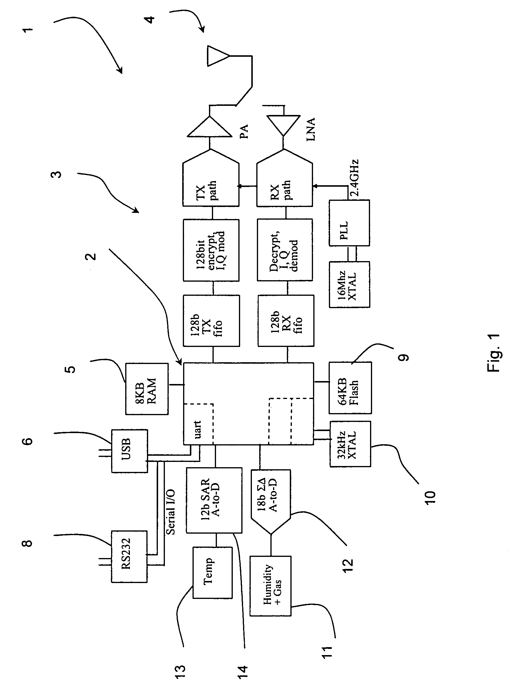
[0052]FIG. 1 is a block diagram of a single-chip wireless sensor device of the invention;

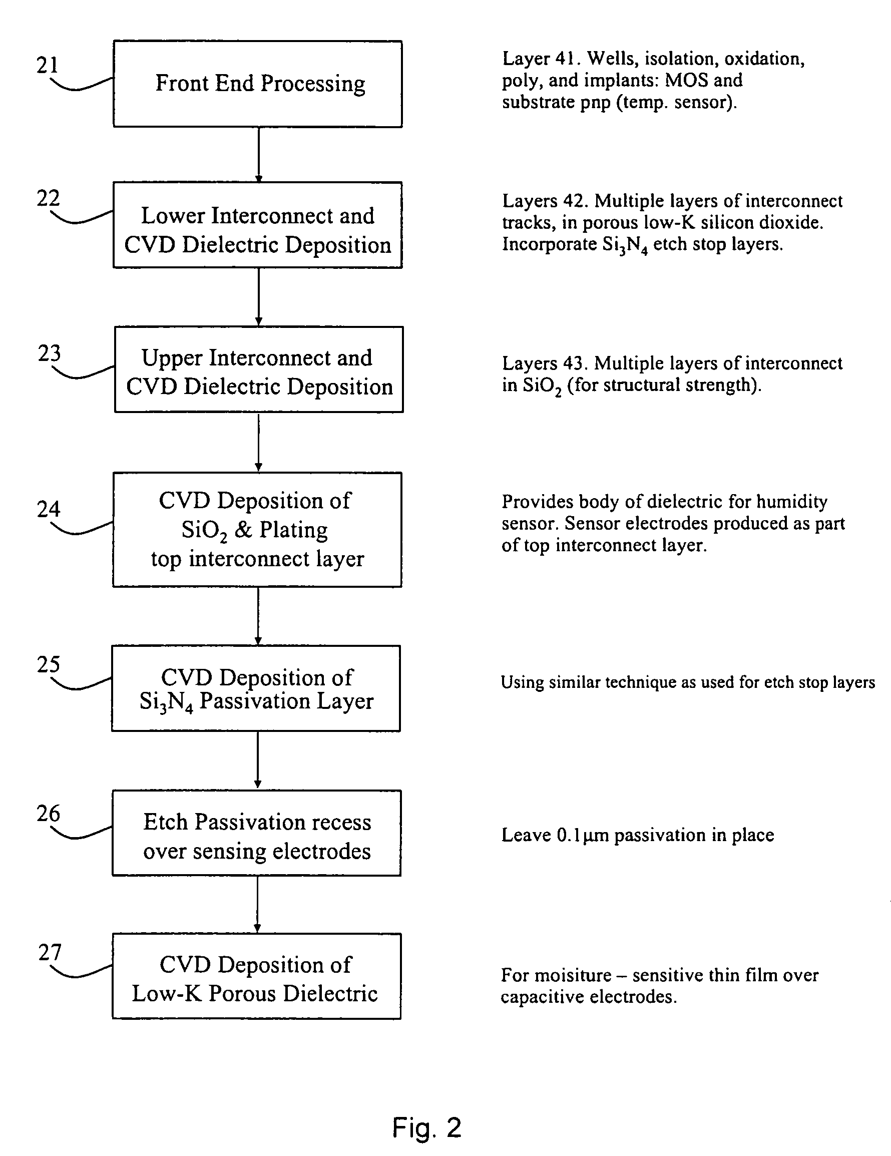
[0053]FIG. 2 is a flow diagram illustrating a process for producing the device;

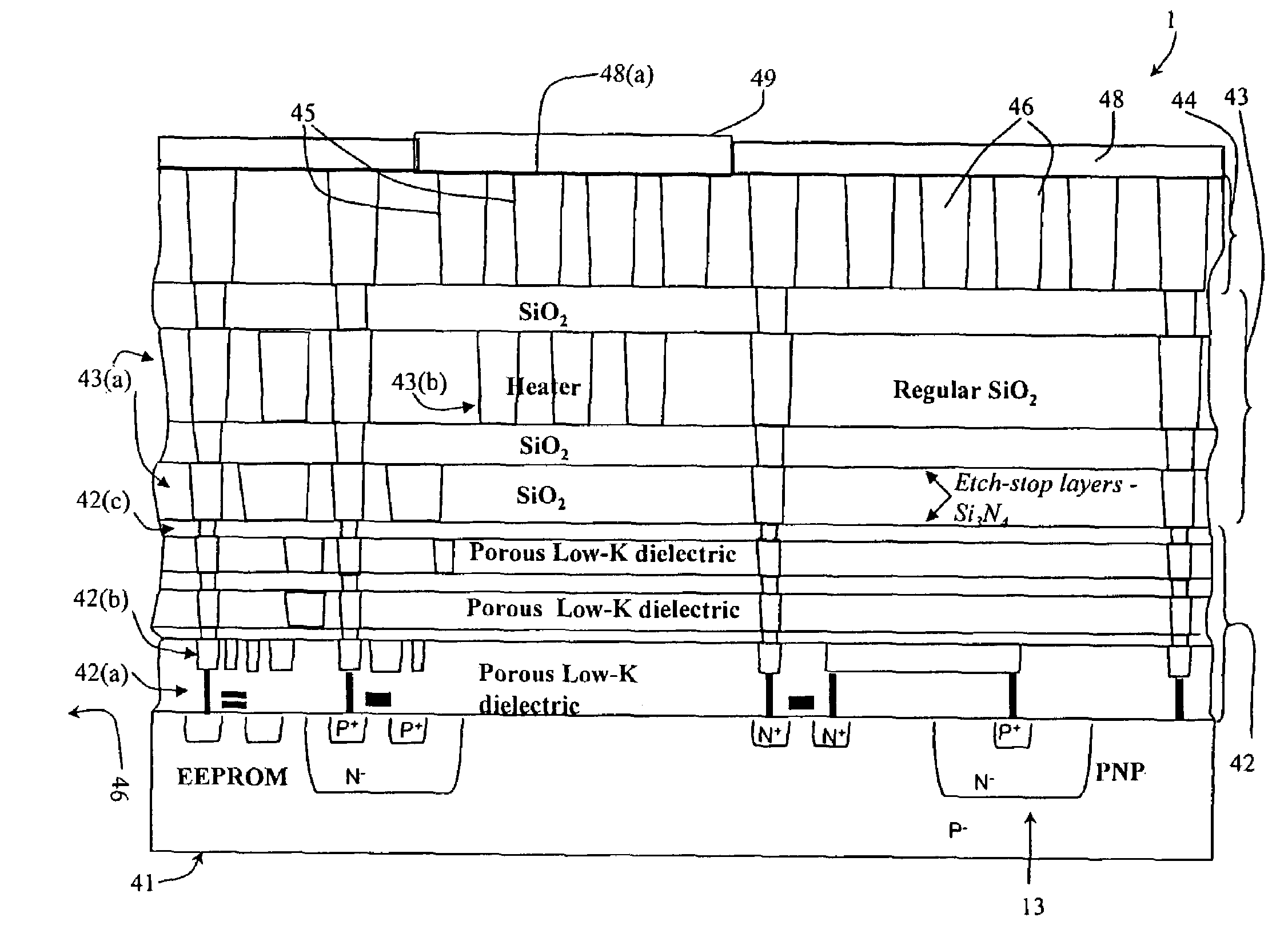
[0054]FIG. 3(a) is a cross-sectional view of the device, FIG. 3(b) is a plan view of sensing electrodes; and FIG. 3(c) is a diagram showing extent of a fringe field between the electrodes;

[0055]FIG. 4 is a schematic of an A-to-D converter of the device;

[0056]FIG. 5 is a diagram showing a sensor component of an alternative embodiment;

[0057]FIGS. 6 and 7 are cross-sectional views of alternative sensor components;

[0058]FIG. 8 is a diagram of a potting arrangement for final packaging;

[0059]FIG. 9 is a circuit diagram of a 12-bit SAR A-to-D converter of the sensor device;

[0060]FIG. 10 is a layout vie...


PUM

PropertyMeasurementUnit
lengthaaaaaaaaaa
capacitanceaaaaaaaaaa
thicknessaaaaaaaaaa

Abstract

A single chip wireless sensor (1) comprises a microcontroller (2) connected by a transmit / receive interface (3) to a wireless antenna (4). The microcontroller (2) is also connected to an 8 kB RAM (5), a USB interface (6), an RS232 interface (8), 64 kB flash memory (9), and a 32 kHz crystal (10). The device (1) senses humidity and temperature, and a humidity sensor (11) is connected by an 18 bit ΣΔ A-to-D converter (12) to the microcontroller (2) and a temperature sensor (13) is connected by a 12 bit SAR A-to-D converter (14) to the microcontroller (2). The device (1) is an integrated chip manufactured in a single process in which both the electronics and sensor components are manufactured using standard CMOS processing techniques, applied to achieve both electronic and sensing components in an integrated process.

Description

[0001]This is a complete application claiming benefit of U.S. Provisional 60 / 558,565 filed Apr. 2, 2004.FIELD OF THE INVENTION[0002]The invention relates to electronic sensors.PRIOR ART DISCUSSION[0003]One of the main driving forces in the electronics industry is the desire to achieve greater integration of functionality so that production is more automated and per-unit cost reduced. An added benefit is, of course, decreased size and thus higher circuit density. Most importantly, for battery applications, higher integration generally results in lower power, due to reduced parasitic capacitances.[0004]However in the field of sensors, and in particular wireless sensors, greater integration has been slow because of the difficulties encountered in integration of microcontroller, A-to-D converter (ADC), memory, RF transceiver, and sensor elements in the one integrated sensor device. These difficulties have arisen because of incompatibilities of materials processing for the various elemen...

Claims


Application Information

Patent Timeline
Patent Type & Authority Patents(United States)
IPC IPC(8): H01L29/80G01N27/12G01N27/22G01N27/414H01L21/469H01L23/52H01L27/105H01L27/15
CPCG01N27/121G01N27/223H01L27/105H01L27/15H01L2924/0002H01L2924/00G01N27/22H01L27/0629H01L23/528
Inventor CUMMINS, TIMOTHY
Owner SILICON LAB INC
Why Eureka
Try Eureka