Semiconductor integrated circuit device comprising MOS transistor having charge storage layer and method for testing semiconductor memory device
a technology of integrated circuit and semiconductor memory, which is applied in the direction of digital storage, measurement devices, instruments, etc., can solve the problems of difficult to search for isolated bits by conventional inspection methods, memory cell reliability often degrades, and it is difficult to enable all memory cells to be produced in the same condition
- Summary
- Abstract
- Description
- Claims
- Application Information
AI Technical Summary
Benefits of technology
Problems solved by technology
Method used
Image


Examples
first embodiment
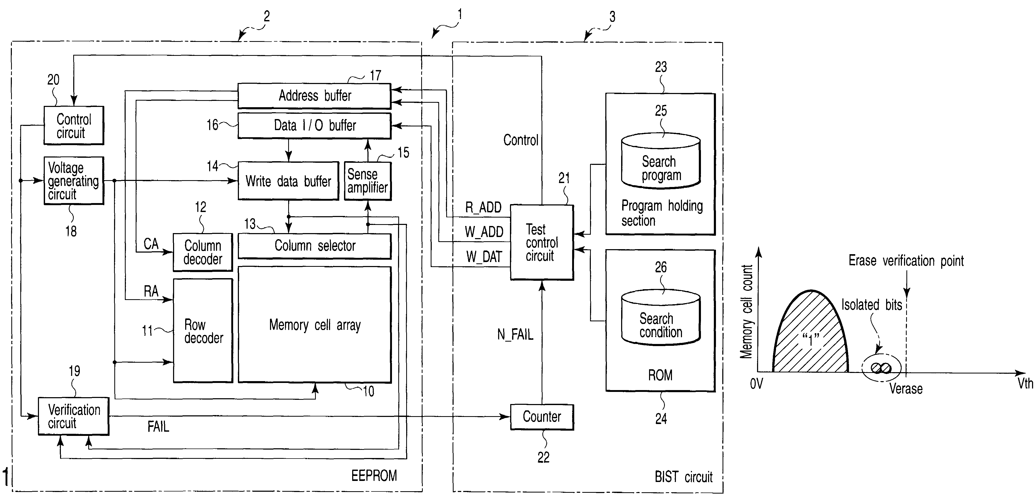
[0043]Description will be given of a semiconductor integrated circuit device and a method for testing a semiconductor memory device in accordance with a first embodiment of the present invention. FIG. 1 is a block diagram of LSI in accordance with the present embodiment.
[0044]As shown in FIG. 1, LSI 1 includes EEPROM 2 and a BIST circuit 3. EEPROM 2 is, for example, a NOR flash memory and stores data. The BIST circuit 3 controls test operations in EEPROM 2.
[0045]First, the configuration of EEPROM 2 will be described. As shown in FIG. 1, EEPROM 2 includes a memory cell array 10, a row decoder 11, a column decoder 12, a column selector 13, a write data buffer 14, a sense amplifier 15, a data I / O buffer 16, an address buffer 17, a voltage generating circuit 18, a verification circuit 19, and a control circuit 20.
[0046]The memory cell array 10 includes a plurality of NOR flash memory cells arranged in a matrix. Each of the memory cells is connected to a bit line, a word line, and a sour...
second embodiment
[0090]Now, description will be given of a semiconductor integrated circuit device and a method for testing a semiconductor memory device in accordance with a second embodiment of the present invention. The present embodiment corresponds to the method for searching for isolated bits in accordance with the first embodiment wherein the isolated bits have threshold voltages lower than those included in the population distribution. FIG. 16 is a block diagram of LSI in accordance with the present embodiment.
[0091]As shown in FIG. 16, the configuration of LSI 1 is almost the same as that in the first embodiment. Thus, only differences from the configuration in accordance with the first embodiment will be described below.
[0092]First, upon determining that a memory cell is normal, the verification circuit 19 in EEPROM 2 outputs the pass signal PASS to the BIST circuit 3. The counter 22 counts the number of pass signals PASS output by the verification circuit 19. That is, the counter 22 count...
third embodiment
[0107]Now, description will be given of a semiconductor integrated circuit device and a method for testing a semiconductor memory device in accordance with a third embodiment of the present invention. The description of the second embodiment relates to the method for searching for isolated bits for which threshold voltages in the erase state are lower than those included in the population distribution. The present embodiment relates to a method for searching for isolated bits for which threshold voltages in a data write state (the memory cells hold binary 0 data) are lower than those included in the population distribution.
[0108]The configuration of LSI 1 in accordance with the present embodiment is as shown in FIG. 16, described in the second embodiment. The search condition is as shown in FIGS. 8 to 10. The verification end voltage is lower than the verification start voltage as is the case with the second embodiment. The other arrangements and operations are similar to those in t...
PUM
 Abstract
Description
Claims
Application Information
 - R&D
- Intellectual Property
- Life Sciences
- Materials
- Tech Scout
- Unparalleled Data Quality
- Higher Quality Content
- 60% Fewer Hallucinations
Browse by: Latest US Patents, China's latest patents, Technical Efficacy Thesaurus, Application Domain, Technology Topic, Popular Technical Reports.
© 2025 PatSnap. All rights reserved.Legal|Privacy policy|Modern Slavery Act Transparency Statement|Sitemap|About US| Contact US: help@patsnap.com