Memory interface optimized for stacked configurations

US7579683B1Active Publication Date: 2009-08-25NAT SEMICON CORP

Image

  • Memory interface optimized for stacked configurations
  • Memory interface optimized for stacked configurations
  • Memory interface optimized for stacked configurations

Examples


Embodiment Construction

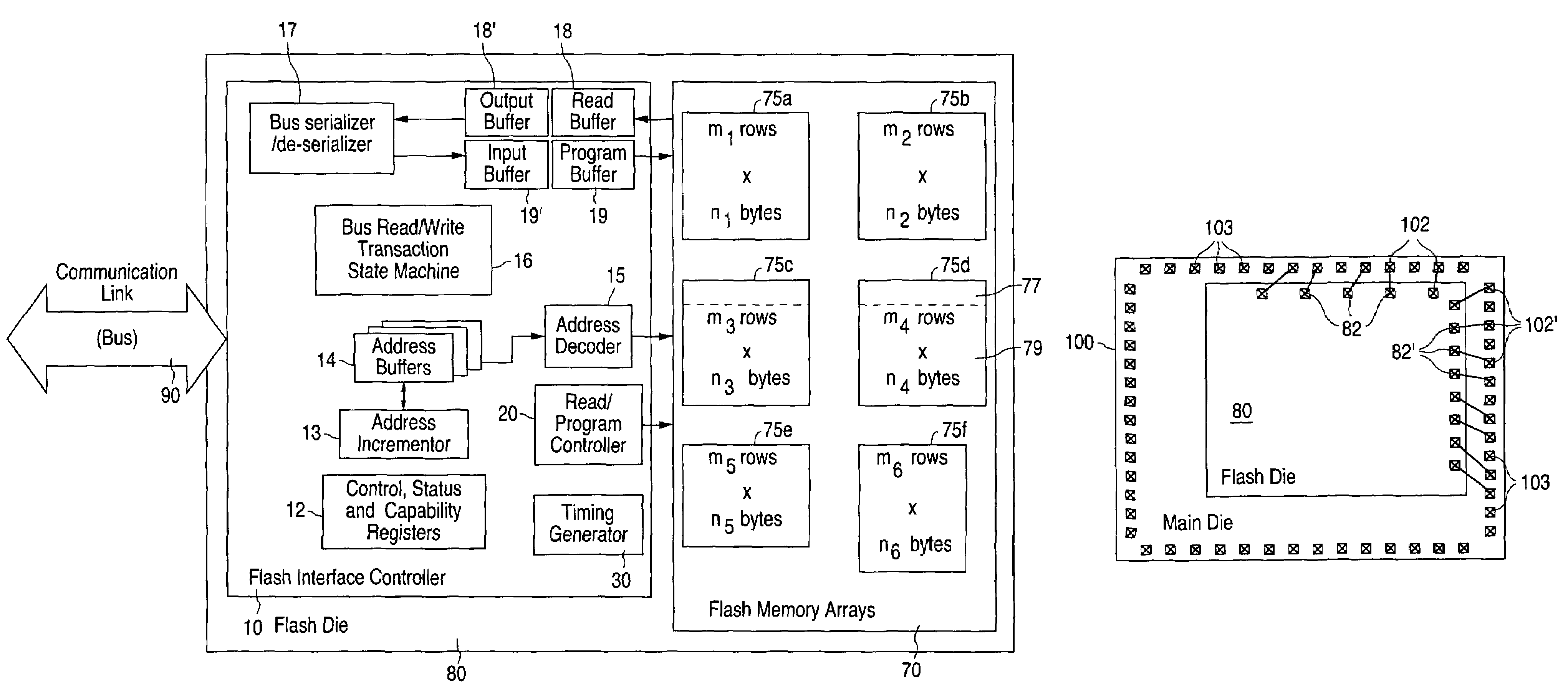
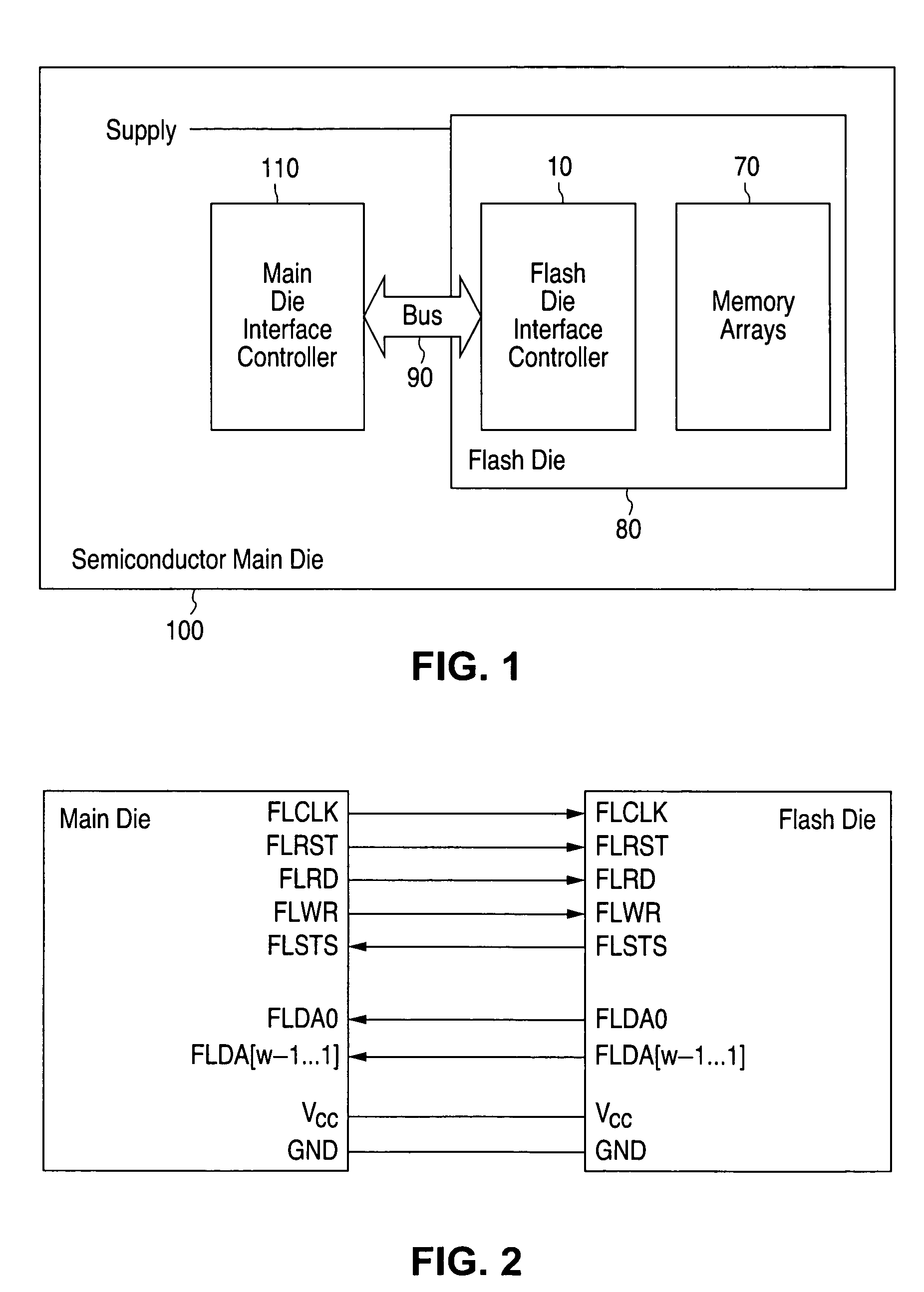
[0041]FIGS. 1 through 10B, discussed below, and the various embodiments used to description the principles of the present invention in this patent document are by way of illustration only and should not be construed in any way to limit the scope of the invention. Those skilled in the art will understand that the principles of the present invention may be implemented in any suitably arranged memory interface system.

[0042]The present invention facilitates designing a connection and communication between a semiconductor device, such as a digital processor, and a nearby memory device, such as a flash memory, by providing a standard interface that is adaptable to a great variety of device types, at either side, to a variety of operational parameters and to a wide range of widths of the communication link between them. The interface enables design of a relatively standard operation program for the semiconductor processing device to efficiently communicate with the memory device, which pro...


PUM


Abstract

A semiconductor die includes a plurality of interconnection pads for connecting with a memory die. The two dies are packaged together in a stacked manner. The plurality of pads are disposed so that the circuit layout of the semiconductor die is invariable with respect to the size of the memory die within a given range of sizes.

Description

CROSS-REFERENCE TO RELATED APPLICATIONS[0001]This application claims the benefit of priority under 35 U.S.C. §119(e)(1) of provisional application Ser. No. 60 / 583,922 filed on Jun. 29, 2004 and provisional application Ser. No. 60 / 583,919 filed Jun. 29, 2004, and provisional application Ser. No. 60 / 583,921 filed Jun. 29, 2004 and provisional application Ser. No. 60 / 583,923 filed Jun. 29, 2004 and provisional application Ser. No. 60 / 583,918 filed Jun. 29, 2004 are incorporated herein by reference for all purposes.[0002]The above application is commonly assigned to the assignee of the present invention. The disclosures of these related patent applications are hereby incorporated by reference for all purposes as if fully set forth herein.TECHNICAL FIELD OF THE INVENTION[0003]This invention relates to communication between semiconductor devices and, in particular, to an interface between a main die and a memory die.BACKGROUND OF THE INVENTION[0004]It is generally known to interconnect tw...

Claims


Application Information

Patent Timeline
25 Aug 2009
Publication
US7579683B1
IPC
H01L23/48
CPC
G11C5/02; H01L25/0657; H01L24/05; H01L2224/48145; H01L2924/01087; H01L2225/06562; H01L2924/14; H01L2924/19043
Inventors
FALIK, OHAD; MELINOVITCH, AVIV