Lighting device and display device provided with the same

a technology of lighting device and display device, which is applied in the direction of lighting and heating apparatus, planar/plate-like light guides, instruments, etc., can solve the problems of difficult to achieve high luminance, difficult to realize lcd modules with excellent color reproducibility, and limited light components with a wavelength range of 600 nm or more, etc., to achieve easy independent adjustment of individual lighting devices, improve temperature-luminance characteristics and reliability, and increase light emitting efficiency of lighting devices

Active Publication Date: 2009-09-01
DAWNCREST IP LLC
View PDF3 Cites 30 Cited by
  • Summary
  • Abstract
  • Description
  • Claims
  • Application Information

AI Technical Summary

Benefits of technology

[0010]In view of the above-mentioned circumstances, the present invention provides a lighting device, which surface-emits light emitted from a light emitting element by using a light guide member. The lighting device includes: a first wavelength conversion member which is provided in an optical path between the light emitting element and a light emitting surface of the lighting device; and a second wavelength conversion member which is provided in an optical path between the first wavelength conversion member and the light emitting surface of the lighting member. According to this structure, light emitted by the second wavelength conversion member has a wavelength shorter than that of light emitted by the first wavelength conversion member. In this case, a description is given on the assumption that the first wavelength conversion member is a red phosphor which emits red light through excitation of blue light and the second wavelength conversion member is a green phosphor which emits green light through excitation of blue light. In other words, the lighting device includes: a red phosphor which is provided in an optical path between the blue light emitting element and the light emitting surface of the lighting device; and a green phosphor which is provided in an optical path between the red phosphor and the light emitting surface of the lighting member. With this structure, blue light emitted by the blue light emitting element and red light obtained through the conversion in the red light emitting phosphor are mixed together to produce violet light, and the violet light is further mixed with green light obtained through the conversion in the green light emitting phosphor through blue light excitation, to thereby produce white light. When the white light is produced in the light conversion order as described above, it is not necessary to use light emitted from the green phosphor as exciting light for exciting the red phosphor, which increases light emitting efficiency of the lighting device. Further, the green light emitting phosphor is completely separated from the blue light emitting element, and therefore the green light emitting phosphor and the light emitting element do not chemically affect each other, which leads to an improvement in temperature-luminance characteristics and reliability of the lighting device. It also makes it easy to independently adjust the chromaticity of individual lighting device.
[0012]Alternatively, the lighting device of the present invention includes: a blue light emitting element; a first color conversion member for converting light into red light through blue light excitation; and a second color conversion member, which is provided independently of the first color conversion member, for converting light into green light through blue light excitation, in which the first color conversion member and the second color conversion member are arranged in an optical path between the light emitting element and a light emitting surface of the lighting device, in a manner that makes a distance between the first color conversion member and the light emitting element shorter than a distance between the second color conversion member and the light emitting element.

Problems solved by technology

However, according to a structure in which a red phosphor and a green phosphor are mixed to be applied onto a transparent film as disclosed in relation to a conventional technology, light emitted from the green phosphor is used to excite the red phosphor, or an in-plane particle density increases, which leads to a problem in that it is difficult to attain high luminance.
Meanwhile, according to additive mixture of two colors respectively obtained from a blue LED and a YAG phosphor (so-called “pseudo white LED” structure), light components with a wavelength range of 600 nm or more are scarce, which hinders realization of an LCD module excellent in color reproducibility.
In general, according to a current color filter technology, it is regarded as being extremely difficult to exceed the NTSC ratio of 100% by using the pseudo white LED as a light source.
It is difficult to adjust colors of the backlight for individual LCD panel by controlling an additive amount of phosphors to be potted into the LED.
Accordingly, it is not always possible to obtain a light source of optimal chromaticity.

Method used


Image

  • Lighting device and display device provided with the same
  • Lighting device and display device provided with the same
  • Lighting device and display device provided with the same

Examples


example 1

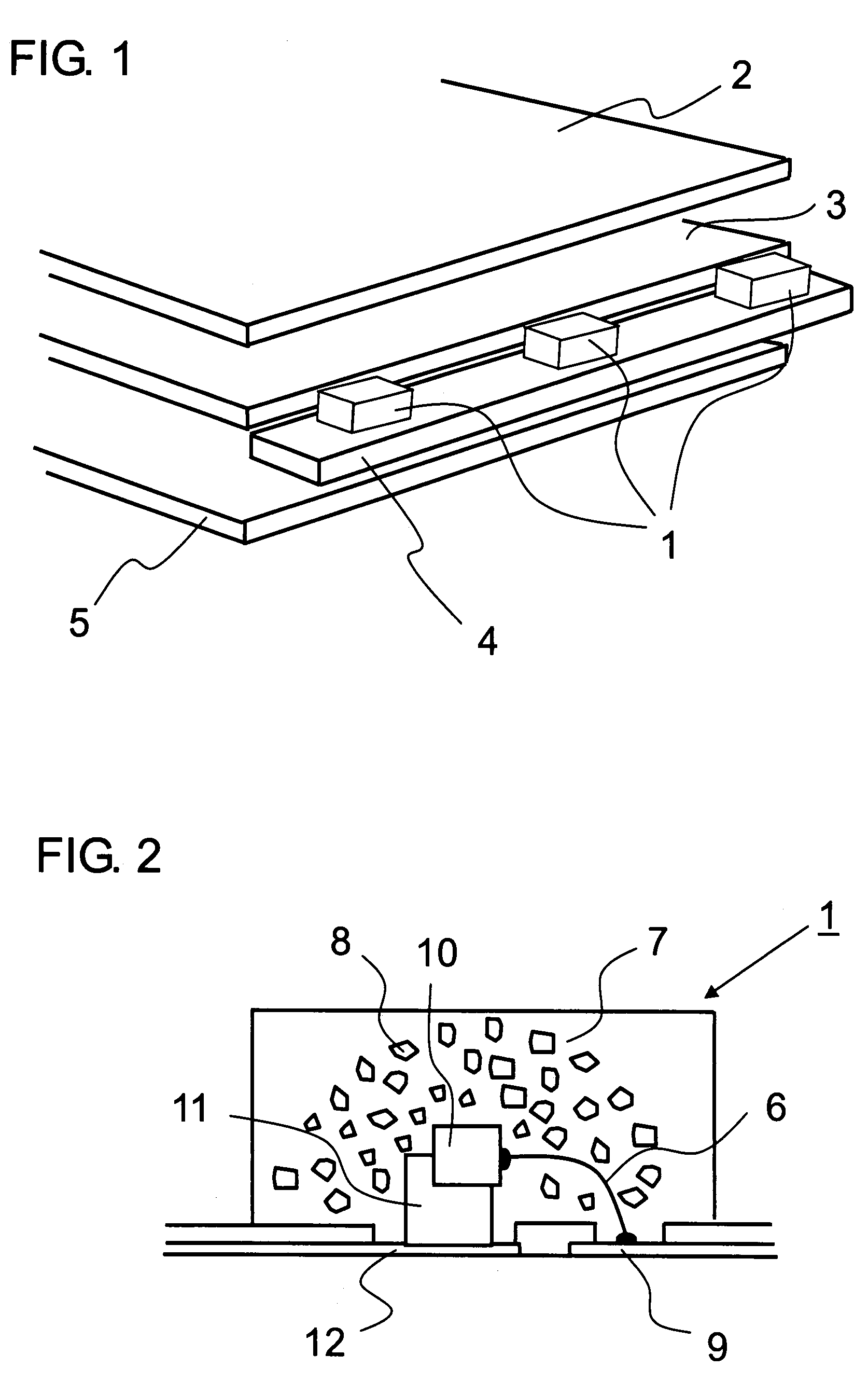
[0044]A lighting device of Example 1 is described with reference to FIGS. 1 and 5. FIG. 1 is a schematic diagram illustrating an outline of the lighting device according to the present invention, and FIG. 5 is a cross-sectional diagram schematically illustrating a structure of a fluorescent film 2. In Example 1, a light emitting diode package 1 is a package for emitting blue light, in which a blue LED element is potted in a resin. As shown in FIG. 1, the light emitting diode package 1 is mounted by being soldered onto a terminal area on a circuit board 4. The light emitting diode package 1 emits one of blue light and ultraviolet light having a spectrum with a peak wavelength ranging from 360 nm to 480 nm. The light emitted from the light emitting diode package 1 is repeatedly reflected and refracted between a light guide member 3 and a reflecting plate 5, so as to be uniformly emitted through a light exiting surface of the light guide member 3. The light emitted from the light guide...

example 2

[0047]Example 2 is described with reference to FIGS. 1 and 6. Example 2 is different from Example 1 in terms of a layer structure of the fluorescent film 2. In Example 1, the resin in which the green phosphor grains 16 and the transparent diffusion beads 17 are mixed and the red phosphor grains 20 are arranged so as to interpose the transparent film 19. According to Example 2, the green phosphor grains 16 and the transparent diffusion beads 17 are separated from each other, and the green phosphor grains 16 and the red phosphor grains 20 are provided so as to interpose a transparent resin 18. That is, as shown in FIG. 6, the transparent resin 18 in which the transparent diffusion beads 17 are mixed is applied and cured on an upper surface the transparent film 19 such as PET. Another transparent resin 18 in which the green phosphor grains 16 are mixed is applied and cured on another surface of the transparent film 19 opposite to the upper surface. Further, on the transparent resin 18 ...

example 3

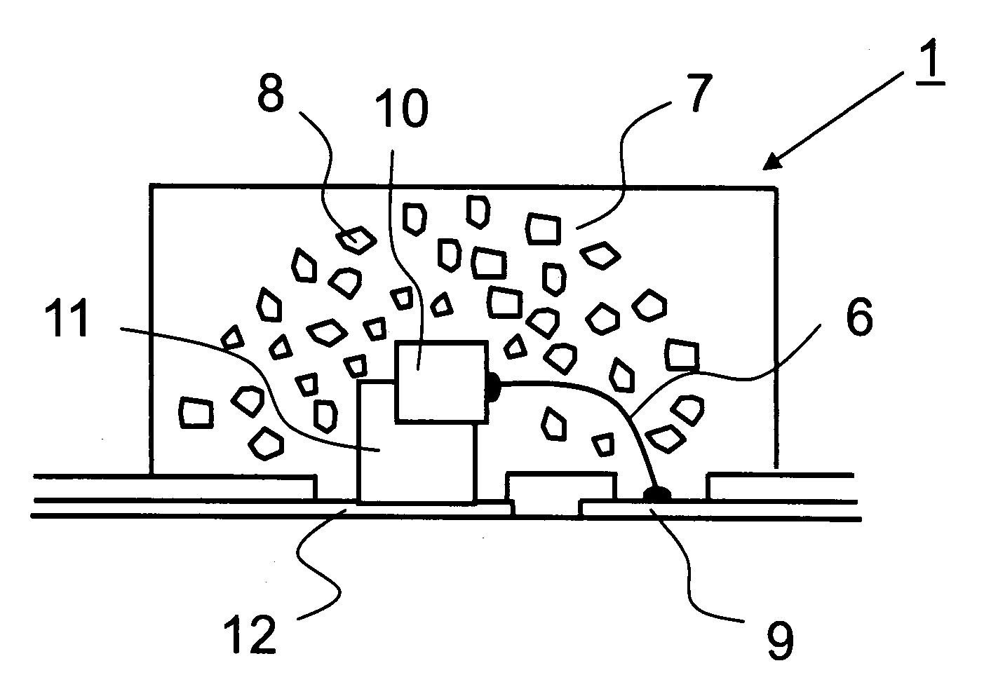
[0048]A lighting device according to Example 3 is described with reference to FIGS. 1 and 2. FIG. 2 is a cross-sectional diagram schematically illustrating a structure of the light emitting diode package 1. Example 3 is different from the aforementioned Examples 1 and 2 in terms of the structure of the light emitting diode package 1. As shown in FIG. 2, the light emitting diode package 1 is structured such that the blue LED element 10 is potted in a resin 7 in which the red phosphor grains 8 are dispersed. As shown in FIG. 1, the light emitting diode package 1 is mounted by being soldered onto a terminal area on the circuit board 4. Therefore, blue light emitted by the blue LED element 10 and red light converted from the blue light through the red phosphor grains 8 exit from the light emitting diode package 1. In other words, the light emitting diode package 1 emits light having a spectrum which includes two wavelengths having peaks each ranging from 450 nm to 480 nm and ranging fro...


PUM


Abstract

A lighting device surface-emits light from a light emitting surface of a light emitting element and guides the emitted light using a light guide member. The lighting device has a first wavelength conversion member for converting light emitted from the light emitting device into light having a first peak wavelength and a second wavelength conversion member for converting light emitted from the light emitting device into light having a wavelength shorter than the first peak wavelength. The first wavelength conversion member is provided between the light emitting element and the light guide member and is contained in a resin potting the light emitting element. A film has a layer containing the second wavelength conversion member. The film is provided on a light emitting surface side of the light guide member.

Description

BACKGROUND OF THE INVENTION[0001]1. Field of the Invention[0002]The present invention relates to a lighting device for illuminating a display element of a non-self light emission type and to a display device used in electronic equipment. In particular, the present invention relates to a liquid crystal display device used in mobile information equipment, a mobile phone, and the like and to a lighting device, such as a front light or a backlight, for illuminating the display element.[0003]2. Description of the Related Art[0004]A display device which has been used in a mobile phone or a mobile computer in recent years often employs a liquid crystal display device capable of obtaining a high-resolution color image with low power consumption. The liquid crystal display device employs a liquid crystal element of a non-self light emission type, and therefore the liquid crystal element is illuminated by using a lighting device having a high-intensity white LED as a light source.[0005]Specif...

Claims


Application Information

Patent Timeline
Patent Type & Authority Patents(United States)
IPC IPC(8): H01L27/15H01L31/12H01L33/00H01L33/50H01L33/58
CPCG02B6/005H01L33/507H01L33/46H01L2224/48091H01L2224/48464H01L2924/00014G02F1/1335
Inventor KURIHARA, MAKOTO
Owner DAWNCREST IP LLC
Why Eureka
Try Eureka