Electron emission device with decreased electrode resistance and fabrication method and electron emission display

a technology of electrode resistance and electron emission display, which is applied in the manufacture of non-electron-emitting shielding screens, electrode systems, electric discharge tubes/lamps, etc., can solve the problems of short circuit of gate electrodes, reduced accuracy, and more power consumption of electron emission displays

Inactive Publication Date: 2009-09-08
SAMSUNG SDI CO LTD
View PDF23 Cites 7 Cited by
  • Summary
  • Abstract
  • Description
  • Claims
  • Application Information

AI Technical Summary

Benefits of technology

[0015]Accordingly, it is an aspect of the present invention to provide an electron emission device of an electron emission display, which decreases electrode resistance without using an ITO electrode.
[0016]Another aspect of the present invention is to provide an electron emission device of an electron emission display, which can employ an inexpensive glass substrate in lieu of an expensive optical transparent glass substrate.

Problems solved by technology

In the thick film process, there are problems in that the electron emission region is not accurately aligned and the height of the printing pattern is irregular, thereby short circuiting the gate electrodes due to the reduced accuracy.
In addition to the problem, the higher the voltage supplied to the cathode electrode, the more power the electron emission display consumes.
Furthermore, the rear exposure process is used in the method of fabricating the cathode substrate of the electron emission display, so that an expensive glass substrate such as a PD200 ITO glass must be employed.
Since the expensive glass substrate must be employed, there arises a problem in that the production cost of the electron emission display is increased.

Method used


Image

  • Electron emission device with decreased electrode resistance and fabrication method and electron emission display
  • Electron emission device with decreased electrode resistance and fabrication method and electron emission display
  • Electron emission device with decreased electrode resistance and fabrication method and electron emission display

Examples


Embodiment Construction

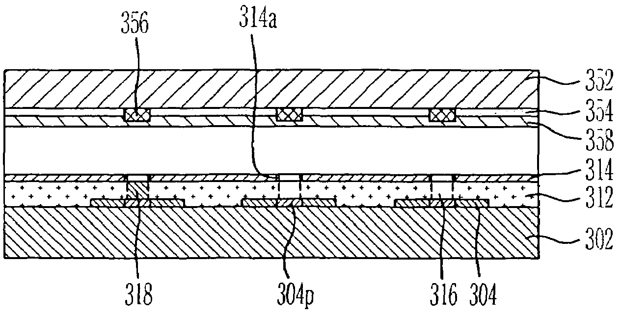
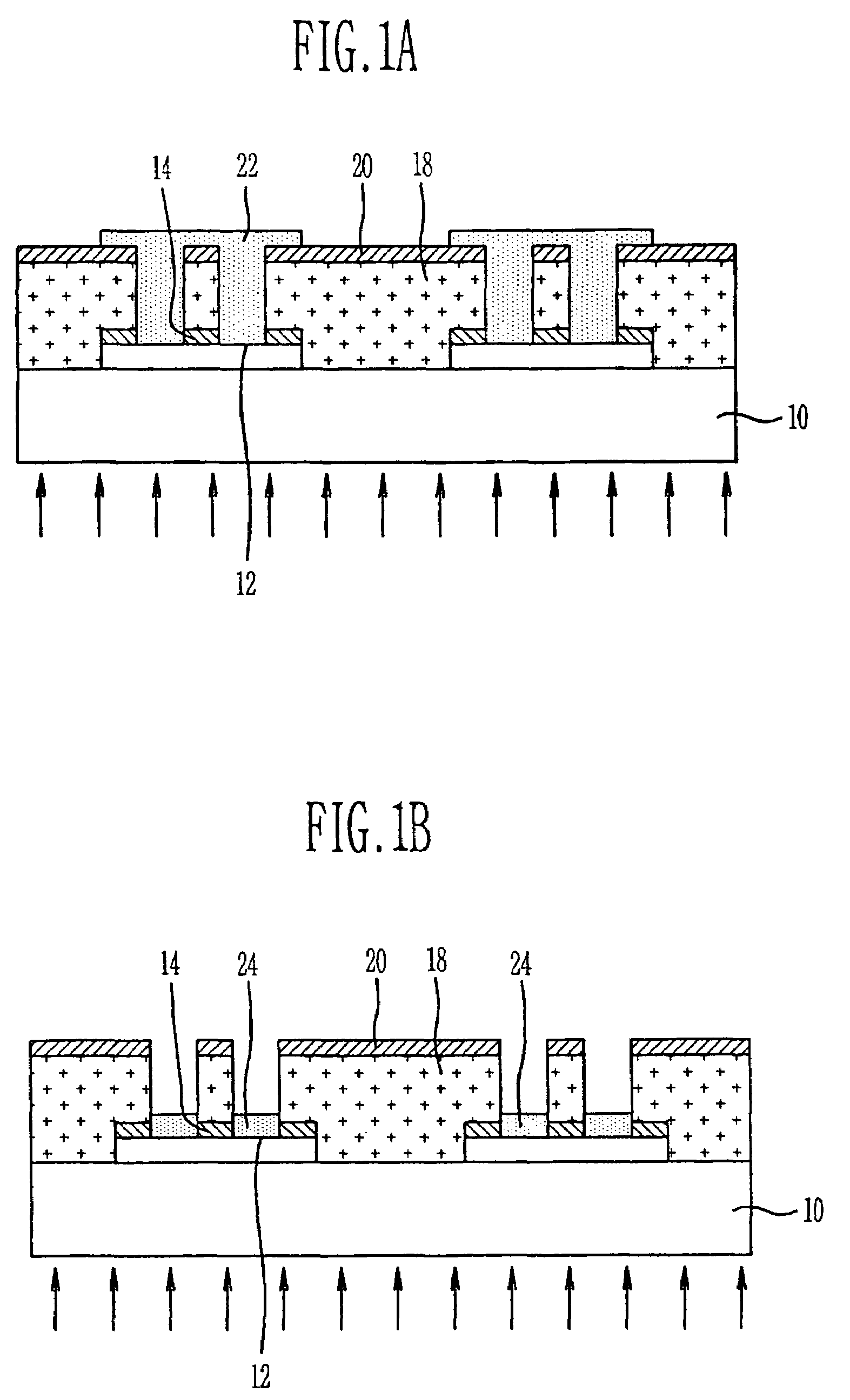
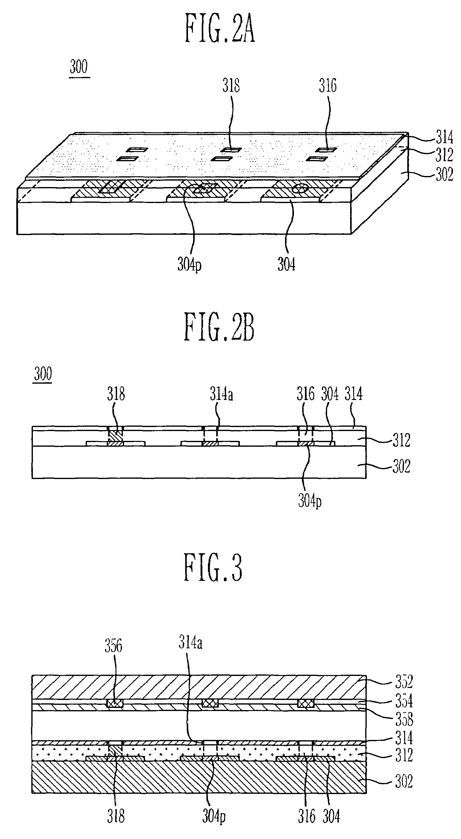
[0044]FIGS. 1A and 1B are sectional views of a method of fabricating an electron emission device.

[0045]Referring to FIGS. 1A and 1B, a transparent Indium Tin Oxide (ITO) electrode 12 is formed on a substrate 10. A stripe electrode 14 is formed In the transparent electrode 12 to have a constant conductivity. Then, a dielectric layer 18 is formed on the substrate 10 having the stripe electrode 14. Then, a gate electrode 20 is formed on the dielectric layer 18. Thereafter, an aperture formed by the transparent electrode 12, the stripe electrode 14 and the dielectric layer 18 on the substrate 10 is filled with a photosensitive material 22, e.g., a Carbon Nano Tube (CNT) paste, and then processed by a rear exposure process as depicted in FIG. 1A. After the rear exposure process, as shown in FIG. 1B, the photosensitive material 22 is developed and dried, thereby forming an electron emission region 24.

[0046]Exemplary embodiments according to the present invention are described in detail be...


PUM


Abstract

An electron emission device includes: a substrate; first and second electrodes insulated from each other and having a predetermined shape on the substrate, at least one of the first and second electrodes being formed with a fine mesh pattern; and an electron emission region formed on the substrate and connected to one of the first and second electrodes. Furthermore, an electron emission display includes: first and second substrate arranged opposite to each other; first and second electrodes insulated from each other and having a predetermined shape on the first substrate, at least one of the first and second electrodes being formed with a fine mesh pattern; an electron emission region formed on the first substrate and connected to one of the first and second electrodes; and an image displaying portion including an anode electrode and a fluorescent layer arranged on the second substrate.

Description

CLAIM OF PRIORITY[0001]This application makes reference to, incorporates the same herein, and claims all benefits accruing under 35 U.S.C. 119 from an application for CATHODE PLATE OF ELECTRON EMISSION DISPLAY AND METHOD FOR MANUFACTURING THE SAME earlier filed in the Korean Intellectual Property Office on 31 Mar. 2004, and there duly assigned Serial No. 2004-21938.BACKGROUND OF THE INVENTION[0002]1. Field of the Invention[0003]The present invention relates to an electron emission device, its fabrication method, and an electron emission display including the electron emission device.[0004]2. Discussion of Related Art[0005]Generally, an electron emission device is classified as either a hot cathode type or a cold cathode type, wherein the hot cathode type and the cold cathode type employ a hot cathode and cold cathode as an electron emission source. A cold cathode type electron emission device comprises a structure, such as a Field Emitter Array (FEA), a Surface Conduction Emitter (S...

Claims


Application Information

Patent Timeline
Patent Type & Authority Patents(United States)
IPC IPC(8): H01J1/46H01J1/52H01J17/04H01J17/12H01J19/38H01J19/40H01J21/10H01J1/30
CPCH01J9/025H01J3/022C01B32/158H01J1/30
Inventor JUNG, KYU-WONKIM, IL-HWAN
Owner SAMSUNG SDI CO LTD
Why Eureka
Try Eureka