

Light emitting diodes with reflective electrode and side electrode
a technology of reflective electrodes and diodes, which is applied in the direction of semiconductor devices, electrical appliances, basic electric elements, etc., can solve the problems of significant number of defects introduced into the semiconducting layer, difficulty in subsequent processing, and high cost and limitation of efforts, so as to achieve real depth tolerance, prevent cracking and chipping, and be sufficiently robust
- Summary
- Abstract
- Description
- Claims
- Application Information
AI Technical Summary
Benefits of technology
Problems solved by technology
Method used
Image

Examples
Embodiment Construction
[0043]The preferred embodiments of the present invention will be better understood by those skilled in the art by reference to the above figures. The preferred embodiments of this invention illustrated in the figures are not intended to be exhaustive or to limit the invention to the precise form disclosed. The figures are chosen to describe or to best explain the principles of the invention and its applicable and practical use to thereby enable others skilled in the art to best utilize the invention.
[0044]The figures are not drawn to scale. In particular, the thickness dimension is expanded relative to the length and width dimensions in order to clearly illustrate the multiple layers of the devices.
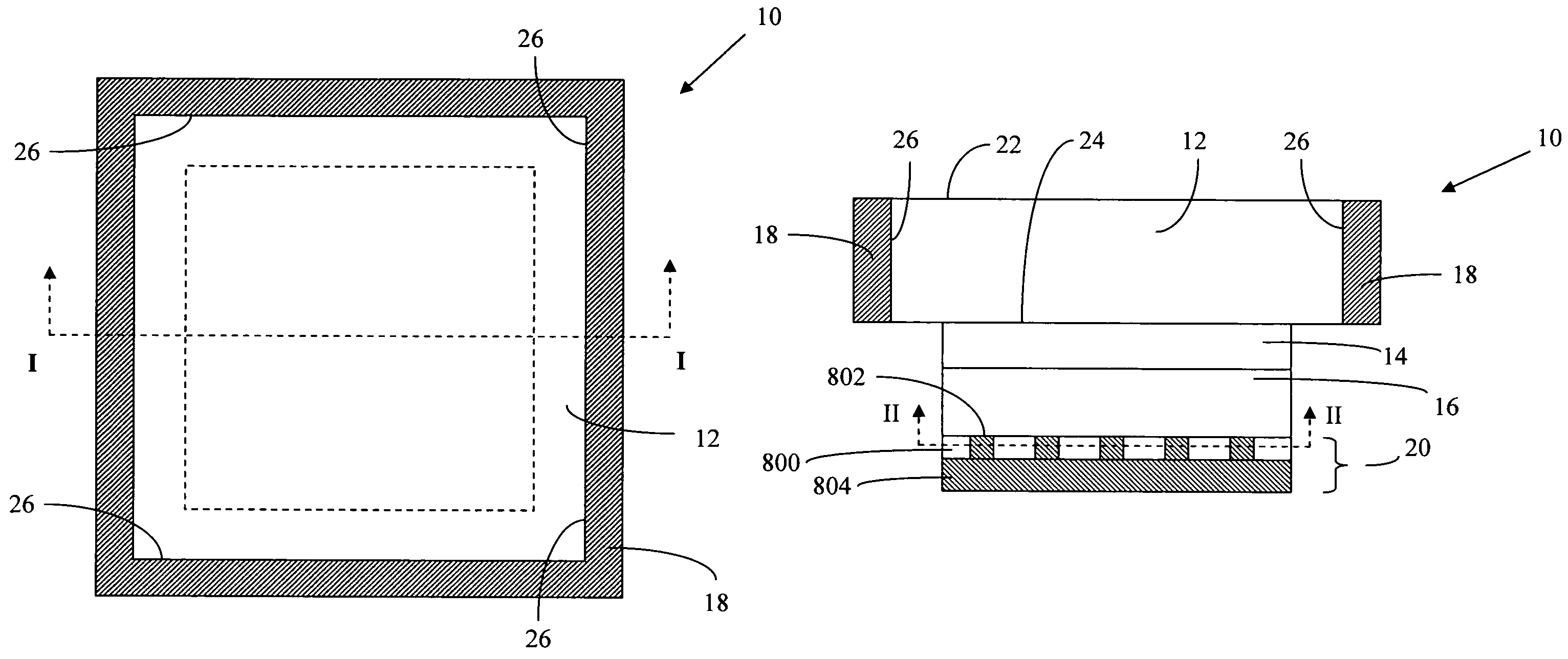
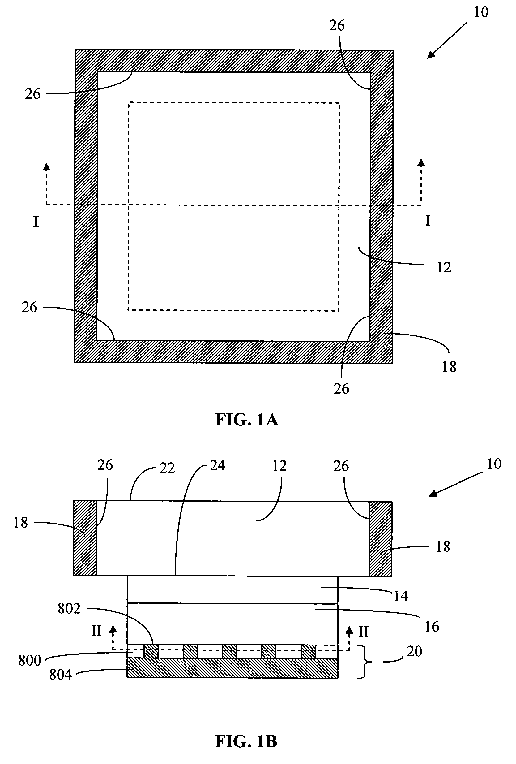
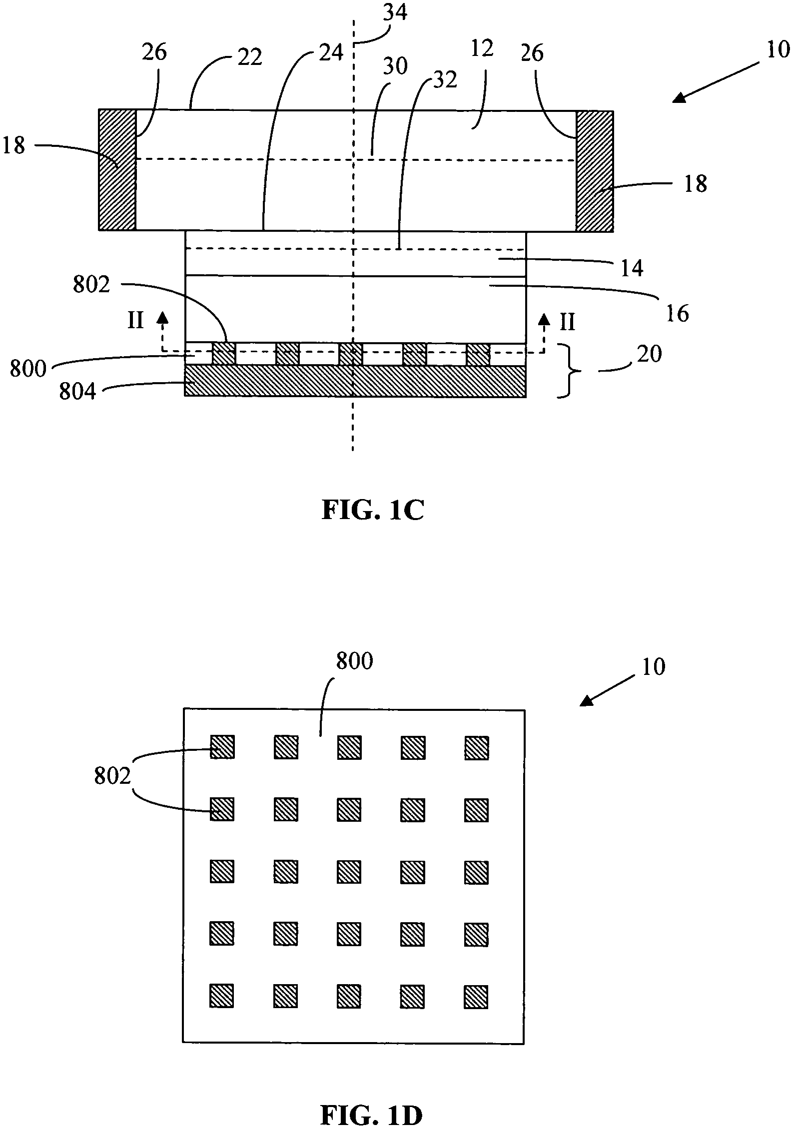
[0045]FIGS. 1A-1I illustrate one embodiment of this invention. FIG. 1A illustrates a top plane view of a light emitting diode 10 of this invention. FIG. 1B is a cross-sectional view along the I-I plane of the light emitting diode 10 illustrated in FIG. 1A. FIG. 1C is another cross-section...
PUM
 Abstract
Description
Claims
Application Information